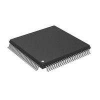
ADSP-2187LKSTZ-210 Analog Devices Inc, ADSP-2187LKSTZ-210 Datasheet - Page 12

ADSP-2187LKSTZ-210
Manufacturer Part Number
ADSP-2187LKSTZ-210
Description
IC DSP CONTRLR 16BIT 100-TQFP
Manufacturer
Analog Devices Inc
Series
ADSP-21xxr
Type
Fixed Pointr
Datasheet
1.ADSP-2184LBSTZ-160.pdf
(48 pages)
Specifications of ADSP-2187LKSTZ-210
Interface
Host Interface, Serial Port
Clock Rate
52MHz
Non-volatile Memory
External
On-chip Ram
160kB
Voltage - I/o
3.30V
Voltage - Core
3.30V
Operating Temperature
0°C ~ 70°C
Mounting Type
Surface Mount
Package / Case
100-TQFP, 100-VQFP
Device Core Size
16b
Format
Fixed Point
Clock Freq (max)
52.5MHz
Mips
52.5
Device Input Clock Speed
52.5MHz
Ram Size
160KB
Program Memory Size
Not RequiredKB
Operating Supply Voltage (typ)
3.3V
Operating Supply Voltage (min)
3V
Operating Supply Voltage (max)
3.6V
Operating Temp Range
0C to 70C
Operating Temperature Classification
Commercial
Mounting
Surface Mount
Pin Count
100
Package Type
LQFP
Lead Free Status / RoHS Status
Lead free / RoHS Compliant
Other names
ADSP-2187LKSTZ210
ADSP-2184L/ADSP-2185L/ADSP-2186L/ADSP-2187L
create a destination word, it is transferred to or from on-chip
memory. The transfer takes one DSP cycle. DSP accesses to
external memory have priority over BDMA byte
memory accesses.
The BDMA Context Reset bit (BCR) controls whether the pro-
cessor is held off while the BDMA accesses are occurring.
Setting the BCR bit to 0 allows the processor to continue opera-
tions. Setting the BCR bit to 1 causes the processor to stop
execution while the BDMA accesses are occurring, to clear the
context of the processor, and start execution at address 0 when
the BDMA accesses have completed.
The BDMA overlay bits specify the OVLAY memory blocks to
be accessed for internal memory. Set these bits as indicated in
Figure
Note: BDMA cannot access external overlay memory regions 1
and 2.
The BMWAIT field, which has 3 bits on ADSP-218xL series
members, allows selection of up to 7 wait states for BDMA
transfers.
Internal Memory DMA Port (IDMA Port; Host Memory
Mode)
The IDMA Port provides an efficient means of communication
between a host system and ADSP-218xL series members. The
port is used to access the on-chip program memory and data
memory of the DSP with only one DSP cycle per word over-
head. The IDMA port cannot, however, be used to write to the
DSP’s memory-mapped control registers. A typical IDMA
transfer process is shown as follows:
1. Host starts IDMA transfer.
2. Host checks IACK control line to see if the DSP is busy.
3. Host uses IS and IAL control lines to latch either the DMA
4. Host uses IS and IRD (or IWR) to read (or write) DSP
5. Host checks IACK line to see if the DSP has completed the
6. Host ends IDMA transfer.
starting address (IDMAA) or the PM/DM OVLAY selec-
tion into the DSP’s IDMA control registers. If Bit 15 = 1,
the values of Bits 7–0 represent the IDMA overlay; Bits
14–8 must be set to 0. If Bit 15 = 0, the value of Bits 13–0
represent the starting address of internal memory to be
accessed and Bit 14 reflects PM or DM for access. Set
IDDMOVLAY and IDPMOVLAY bits in the IDMA over-
lay register as indicted in
internal memory (PM or DM).
previous IDMA operation.
11.
Table
8.
Rev. C | Page 12 of 48 | January 2008
Table 8. IDMA/BDMA Overlay Bits
The IDMA port has a 16-bit multiplexed address and data bus
and supports 24-bit program memory. The IDMA port is com-
pletely asynchronous and can be written while the ADSP-218xL
is operating at full speed.
The DSP memory address is latched and then automatically
incremented after each IDMA transaction. An external device
can therefore access a block of sequentially addressed memory
by specifying only the starting address of the block. This
increases throughput as the address does not have to be sent for
each memory access.
IDMA port access occurs in two phases. The first is the IDMA
Address Latch cycle. When the acknowledge is asserted, a 14-bit
address and 1-bit destination type can be driven onto the bus by
an external device. The address specifies an on-chip memory
location, the destination type specifies whether it is a DM or PM
access. The falling edge of the IDMA address latch signal (IAL)
or the missing edge of the IDMA select signal (IS) latches this
value into the IDMAA register.
Once the address is stored, data can be read from, or written to,
the ADSP-218xL’s on-chip memory. Asserting the select line
(IS) and the appropriate read or write line (IRD and IWR
respectively) signals the ADSP-218xL that a particular transac-
tion is required. In either case, there is a one-processor-cycle
delay for synchronization. The memory access consumes one
additional processor cycle.
Once an access has occurred, the latched address is automati-
cally incremented, and another access can occur.
Through the IDMAA register, the DSP can also specify the
starting address and data format for DMA operation.
Asserting the IDMA port select (IS) and address latch enable
(IAL) directs the ADSP-218xL to write the address onto the
IAD14–0 bus into the IDMA Control Register
15 is set to 0, IDMA latches the address. If Bit 15 is set to 1,
IDMA latches into the OVLAY register. This register, also
shown in
(0x3FE0). Note that the latched address (IDMAA) cannot be
read back by the host. The IDMA Overlay register applies to
The ADSP-2187L processor only.
When Bit 14 in 0x3FE7 is set to zero, short reads use the timing
shown in
1, timing in
Read Only Mode. Set IDDMOVLAY and IDPMOVLAY bits in
the IDMA overlay register as indicated in
ADSP-218x DSP Hardware Reference for additional details.
Processor
ADSP-2184L
ADSP-2185L
ADSP-2186L
ADSP-2187L
Figure
Figure 26 on Page
Figure 27 on Page 35
12, is memory-mapped at address DM
IDMA/BDMA
PMOVLAY
0
0
0
0, 4, 5
34. When Bit 14 in 0x3FE7 is set to
applies for short reads in Short
Table
IDMA/BDMA
DMOVLAY
0
0
0
0, 4, 5
(Figure
8. Refer to the
12). If Bit


