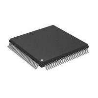
ADSP-2187LKSTZ-210 Analog Devices Inc, ADSP-2187LKSTZ-210 Datasheet - Page 18

ADSP-2187LKSTZ-210
Manufacturer Part Number
ADSP-2187LKSTZ-210
Description
IC DSP CONTRLR 16BIT 100-TQFP
Manufacturer
Analog Devices Inc
Series
ADSP-21xxr
Type
Fixed Pointr
Datasheet
1.ADSP-2184LBSTZ-160.pdf
(48 pages)
Specifications of ADSP-2187LKSTZ-210
Interface
Host Interface, Serial Port
Clock Rate
52MHz
Non-volatile Memory
External
On-chip Ram
160kB
Voltage - I/o
3.30V
Voltage - Core
3.30V
Operating Temperature
0°C ~ 70°C
Mounting Type
Surface Mount
Package / Case
100-TQFP, 100-VQFP
Device Core Size
16b
Format
Fixed Point
Clock Freq (max)
52.5MHz
Mips
52.5
Device Input Clock Speed
52.5MHz
Ram Size
160KB
Program Memory Size
Not RequiredKB
Operating Supply Voltage (typ)
3.3V
Operating Supply Voltage (min)
3V
Operating Supply Voltage (max)
3.6V
Operating Temp Range
0C to 70C
Operating Temperature Classification
Commercial
Mounting
Surface Mount
Pin Count
100
Package Type
LQFP
Lead Free Status / RoHS Status
Lead free / RoHS Compliant
Other names
ADSP-2187LKSTZ210
ADSP-2184L/ADSP-2185L/ADSP-2186L/ADSP-2187L
Table 9. Common-Mode Pins (Continued)
1
2
3
MEMORY INTERFACE PINS
ADSP-218xL series members can be used in one of two modes:
Full Memory Mode, which allows BDMA operation with full
external overlay memory and I/O capability, or Host Mode,
which allows IDMA operation with limited external addressing
capabilities.
Table 10. Full Memory Mode Pins (Mode C = 0)
Table 11. Host Mode Pins (Mode C = 1)
1
2
Pin Name
V
V
GND
EZ-Port
Pin Name
A13–0
D23–0
Pin Name
IAD15–0
A0
D23–8
IWR
IRD
IAL
IS
IACK
Interrupt/Flag pins retain both functions concurrently. If IMASK is set to enable the corresponding interrupts, the DSP will vector to the appropriate interrupt vector address
This mode applies to the ADSP-2187L only.
SPORT configuration determined by the DSP System Control Register. Software configurable.
In Host Mode, external peripheral addresses can be decoded using the A0, CMS, PMS, DMS, and IOMS signals.
Mode D function available on ADSP-2187L only.
when the pin is asserted, either by external devices or set as a programmable flag.
DDINT
DDEXT
No. of Pins
14
24
No. of Pins
1
16
1
1
1
1
1
16
No. of Pins
4
7
20
9
I/O
O
I/O
I/O
I/O
O
I/O
I
I
I
I
O
Function
Address Output Pins for Program, Data, Byte, and I/O Spaces
Data I/O Pins for Program, Data, Byte, and I/O Spaces (8 MSBs are also used as Byte Memory
Addresses.)
Function
IDMA Port Address/Data Bus
Address Pin for External I/O, Program, Data, or Byte Access
Data I/O Pins for Program, Data, Byte, and I/O Spaces
IDMA Write Enable
IDMA Read Enable
IDMA Address Latch Pin
IDMA Select
IDMA Port Acknowledge Configurable in Mode D
I/O
I
I
I
I/O
Rev. C | Page 18 of 48 | January 2008
Function
Internal V
External V
Ground (BGA)
For Emulation Use
DD
DD
(3.3 V) Power (BGA)
(3.3 V) Power (BGA)
The operating mode is determined by the state of the Mode C
pin during RESET and cannot be changed while the processor is
running.
pins of the DSP during either of the two operating modes (Full
Memory or Host). A signal in one table shares a pin with a sig-
nal from the other table, with the active signal determined by
the mode that is set. For the shared pins and their alternate sig-
nals (e.g., A4/IAD3), refer to the package pinouts in
Page 44
and
Table 10
Table 30 on Page
and
2
; Open Drain
Table 11
1
45.
list the active signals at specific
Table 29 on


