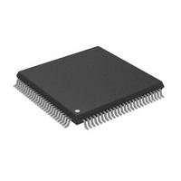
ADSP-2187LKSTZ-210 Analog Devices Inc, ADSP-2187LKSTZ-210 Datasheet - Page 22

ADSP-2187LKSTZ-210
Manufacturer Part Number
ADSP-2187LKSTZ-210
Description
IC DSP CONTRLR 16BIT 100-TQFP
Manufacturer
Analog Devices Inc
Series
ADSP-21xxr
Type
Fixed Pointr
Datasheet
1.ADSP-2184LBSTZ-160.pdf
(48 pages)
Specifications of ADSP-2187LKSTZ-210
Interface
Host Interface, Serial Port
Clock Rate
52MHz
Non-volatile Memory
External
On-chip Ram
160kB
Voltage - I/o
3.30V
Voltage - Core
3.30V
Operating Temperature
0°C ~ 70°C
Mounting Type
Surface Mount
Package / Case
100-TQFP, 100-VQFP
Device Core Size
16b
Format
Fixed Point
Clock Freq (max)
52.5MHz
Mips
52.5
Device Input Clock Speed
52.5MHz
Ram Size
160KB
Program Memory Size
Not RequiredKB
Operating Supply Voltage (typ)
3.3V
Operating Supply Voltage (min)
3V
Operating Supply Voltage (max)
3.6V
Operating Temp Range
0C to 70C
Operating Temperature Classification
Commercial
Mounting
Surface Mount
Pin Count
100
Package Type
LQFP
Lead Free Status / RoHS Status
Lead free / RoHS Compliant
Other names
ADSP-2187LKSTZ210
ADSP-2184L/ADSP-2185L/ADSP-2186L/ADSP-2187L
ABSOLUTE MAXIMUM RATINGS
Stresses greater than those listed below may cause permanent
damage to the device. These are stress ratings only. Functional
operation of the device at these or any other conditions greater
than those indicated in the operational sections of this specifica-
tion is not implied. Exposure to absolute maximum rating
conditions for extended periods may affect device reliability.
1
2
PACKAGE INFORMATION
The information presented in
the package branding for the ADSP-218xL processors. For a
complete listing of product availability, see
Page
Table 13. Package Brand Information
Parameter
Supply Voltage (V
Input Voltage
Output Voltage Swing
Operating Temperature Range
Storage Temperature Range
Brand Key
t
pp
Z
cc
vvvvvv.x
n.n
yyww
Applies to bidirectional pins (D23–0, RFS0, RFS1, SCLK0, SCLK1, TFS0, TFS1,
Applies to output pins (BG, PMS, DMS, BMS, IOMS, CMS, RD, WR, PWDACK,
A13–1, PF7–0) and input only pins (CLKIN, RESET, BR, DR0, DR1, PWD).
A0, DT0, DT1, CLKOUT, FL2–0, BGH).
47.
1
Figure 15. Typical Package Brand
DD
)
yyww country_of_origin
2
a
ADSP-218xL
vvvvvv.x n.n
Field Description
Temperature Range
Package Type
RoHs Compliant Option (optional)
See Ordering Guide
Assembly Lot Code
Silicon Revision
Date Code
tppZ-cc
Figure 15
Rating
–0.3 V to +4.6 V
–0.5 V to V
–0.5 V to V
–40°C to +85°C
–65°C to +150°C
provides details about
Ordering Guide on
DD
DD
Rev. C | Page 22 of 48 | January 2008
+0.5 V
+ 0.5 V
ESD SENSITIVITY
TIMING SPECIFICATIONS
General Notes
Use the exact timing information given. Do not attempt to
derive parameters from the addition or subtraction of others.
While addition or subtraction would yield meaningful results
for an individual device, the values given in this data sheet
reflect statistical variations and worst cases. Consequently,
parameters cannot be added up meaningfully to derive
longer times.
Timing Notes
Switching characteristics specify how the processor changes its
signals. Designers have no control over this timing—circuitry
external to the processor must be designed for compatibility
with these signal characteristics. Switching characteristics tell
what the processor will do in a given circumstance. Switching
characteristics can also be used to ensure that any timing
requirement of a device connected to the processor (such as
memory) is satisfied.
Timing requirements apply to signals that are controlled by cir-
cuitry external to the processor, such as the data input for a read
operation. Timing requirements guarantee that the processor
operates correctly with other devices.
Frequency Dependency For Timing Specifications
t
with a frequency equal to half the instruction rate. For example,
a 26 MHz input clock (which is equivalent to 38 ns) yields a
19 ns processor cycle (equivalent to 52 MHz). t
the range of 0.5 t
timing parameters to obtain the specification value.
Example: t
CK
is defined as 0.5 t
CKH
= 0.5 t
CKI
ESD (electrostatic discharge) sensitive device.
Charged devices and circuit boards can discharge
without detection. Although this product features
patented or proprietary protection circuitry, damage
may occur on devices subjected to high energy ESD.
Therefore, proper ESD precautions should be taken to
avoid performance degradation or loss of functionality.
period should be substituted for all relevant
CKI
CK
. The ADSP-218xL uses an input clock
– 7 ns = 0.5 (19) – 7 ns = 2.5 ns
CK
values within


