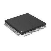
ADSP-2187LKSTZ-210 Analog Devices Inc, ADSP-2187LKSTZ-210 Datasheet - Page 5

ADSP-2187LKSTZ-210
Manufacturer Part Number
ADSP-2187LKSTZ-210
Description
IC DSP CONTRLR 16BIT 100-TQFP
Manufacturer
Analog Devices Inc
Series
ADSP-21xxr
Type
Fixed Pointr
Datasheet
1.ADSP-2184LBSTZ-160.pdf
(48 pages)
Specifications of ADSP-2187LKSTZ-210
Interface
Host Interface, Serial Port
Clock Rate
52MHz
Non-volatile Memory
External
On-chip Ram
160kB
Voltage - I/o
3.30V
Voltage - Core
3.30V
Operating Temperature
0°C ~ 70°C
Mounting Type
Surface Mount
Package / Case
100-TQFP, 100-VQFP
Device Core Size
16b
Format
Fixed Point
Clock Freq (max)
52.5MHz
Mips
52.5
Device Input Clock Speed
52.5MHz
Ram Size
160KB
Program Memory Size
Not RequiredKB
Operating Supply Voltage (typ)
3.3V
Operating Supply Voltage (min)
3V
Operating Supply Voltage (max)
3.6V
Operating Temp Range
0C to 70C
Operating Temperature Classification
Commercial
Mounting
Surface Mount
Pin Count
100
Package Type
LQFP
Lead Free Status / RoHS Status
Lead free / RoHS Compliant
Other names
ADSP-2187LKSTZ210
Table 2. Modes of Operation
1
2
during power-down, reconfigure PF2 to be an input, as the pull-
up or pull-down resistance will hold the pin in a known state,
and will not switch.
Active Configuration
Active Configuration involves the use of a three-statable exter-
nal driver connected to the Mode C pin. A driver’s output
enable should be connected to the DSP’s RESET signal such that
it only drives the PF2 pin when RESET is active (low). When
RESET is deasserted, the driver should be three-state, thus
allowing full use of the PF2 pin as either an input or output. To
minimize power consumption during power-down, configure
the programmable flag as an output when connected to a three-
stated buffer. This ensures that the pin will be held at a constant
level, and will not oscillate should the three-state driver’s level
hover around the logic switching point.
IDMA ACK Configuration (ADSP-2187L Only)
Mode D = 0 and in Host Mode: IACK is an active, driven signal
and cannot be “wire-OR’ed.” Mode D = 1 and in Host Mode:
IACK is an open drain and requires an external pull-down, but
multiple IACK pins can be “wire-OR’ed” together.
INTERRUPTS
The interrupt controller allows the processor to respond to the
eleven possible interrupts and reset with minimum overhead.
ADSP-218xL series members provide four dedicated external
interrupt input pins: IRQ2, IRQL0, IRQL1, and IRQE (shared
with the PF7–4 pins). In addition, SPORT1 may be reconfig-
ured for IRQ0, IRQ1, FI, and FO, for a total of six external
interrupts. The ADSP-218xL also supports internal interrupts
Mode D
X
X
0
0
1
1
Mode D applies to the ADSP-2187L processor only.
Considered as standard operating settings. Using these configurations allows for easier design and better memory management.
1
Mode C
0
0
1
1
1
1
Mode B
0
1
0
0
0
0
Mode A
0
0
0
1
0
1
ADSP-2184L/ADSP-2185L/ADSP-2186L/ADSP-2187L
Rev. C | Page 5 of 48 | January 2008
Booting Method
BDMA feature is used to load the first 32 program memory words from the byte memory
space. Program execution is held off until all 32 words have been loaded. Chip is
configured in Full Memory Mode.
No automatic boot operations occur. Program execution starts at external memory
location 0. Chip is configured in Full Memory Mode. BDMA can still be used, but the
processor does not automatically use or wait for these operations.
BDMA feature is used to load the first 32 program memory words from the byte memory
space. Program execution is held off until all 32 words have been loaded. Chip is
configured in Host Mode. IACK has active pull-down. (Requires additional hardware.)
IDMA feature is used to load any internal memory as desired. Program execution is held
off until the host writes to internal program memory location 0. Chip is configured in
Host Mode. IACK has active pull-down.
BDMA feature is used to load the first 32 program memory words from the byte memory
space. Program execution is held off until all 32 words have been loaded. Chip is
configured in Host Mode; IACK requires external pull-down. (Requires additional
hardware.)
IDMA feature is used to load any internal memory as desired. Program execution is held
off until the host writes to internal program memory location 0. Chip is configured in
Host Mode. IACK requires external pull-down.
from the timer, the byte DMA port, the two serial ports, soft-
ware, and the power-down control circuit. The interrupt levels
are internally prioritized and individually maskable (except
power-down and reset). The IRQ2, IRQ0, and IRQ1 input pins
can be programmed to be either level- or edge-sensitive. IRQL0
and IRQL1 are level-sensitive and IRQE is edge-sensitive. The
priorities and vector addresses of all interrupts are shown in
Table
Table 3. Interrupt Priority and Interrupt Vector Addresses
Interrupt routines can either be nested with higher priority
interrupts taking precedence or processed sequentially. Inter-
rupts can be masked or unmasked with the IMASK register.
Source Of Interrupt
RESET (or Power-Up with PUCR = 1) 0x0000 (highest priority)
Power-Down (Nonmaskable)
IRQ2
IRQL1
IRQL0
SPORT0 Transmit
SPORT0 Receive
IRQE
BDMA Interrupt
SPORT1 Transmit or IRQ1
SPORT1 Receive or IRQ0
Timer
3.
2
2
2
Interrupt Vector Address
(Hex)
0x002C
0x0004
0x0008
0x000C
0x0010
0x0014
0x0018
0x001C
0x0020
0x0024
0x0028 (lowest priority)


