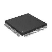
ADSP-2187LKSTZ-210 Analog Devices Inc, ADSP-2187LKSTZ-210 Datasheet - Page 43

ADSP-2187LKSTZ-210
Manufacturer Part Number
ADSP-2187LKSTZ-210
Description
IC DSP CONTRLR 16BIT 100-TQFP
Manufacturer
Analog Devices Inc
Series
ADSP-21xxr
Type
Fixed Pointr
Datasheet
1.ADSP-2184LBSTZ-160.pdf
(48 pages)
Specifications of ADSP-2187LKSTZ-210
Interface
Host Interface, Serial Port
Clock Rate
52MHz
Non-volatile Memory
External
On-chip Ram
160kB
Voltage - I/o
3.30V
Voltage - Core
3.30V
Operating Temperature
0°C ~ 70°C
Mounting Type
Surface Mount
Package / Case
100-TQFP, 100-VQFP
Device Core Size
16b
Format
Fixed Point
Clock Freq (max)
52.5MHz
Mips
52.5
Device Input Clock Speed
52.5MHz
Ram Size
160KB
Program Memory Size
Not RequiredKB
Operating Supply Voltage (typ)
3.3V
Operating Supply Voltage (min)
3V
Operating Supply Voltage (max)
3.6V
Operating Temp Range
0C to 70C
Operating Temperature Classification
Commercial
Mounting
Surface Mount
Pin Count
100
Package Type
LQFP
Lead Free Status / RoHS Status
Lead free / RoHS Compliant
Other names
ADSP-2187LKSTZ210
TEST CONDITIONS
Figure 44
(except output disable/enable).
Output Disable Time
Output pins are considered to be disabled when they have
stopped driving and started a transition from the measured out-
put high or low voltage to a high impedance state. The output
disable time (t
shown in
ence signal reaches a high or low voltage level to when the
output voltages have changed by 0.5 V from the measured out-
put high or low voltage.
The decay time, t
and the current load, i
mated by the following equation:
from which
is calculated. If multiple pins (such as the data bus) are disabled,
the measurement value is that of the last pin to stop driving.
Output Enable Time
Output pins are considered to be enabled when they have made
a transition from a high-impedance state to when they start
driving. The output enable time (t
a reference signal reaches a high or low voltage level to when the
output has reached a specified high or low trip point, as shown
in
the measurement value is that of the first pin to start driving.
Figure 44. Voltage Reference Levels for AC Measurements (Except Output
Figure
OUTPUT
INPUT
OR
45. If multiple pins (such as the data bus) are enabled,
Figure
shows voltage reference levels for all ac measurements
DIS
1.5V
) is the difference of t
45. The time is the interval from when a refer-
DECAY
t
DIS
t
DECAY
L
, is dependent on the capacitive load, C
=
, on the output pin. It can be approxi-
t
Enable/Disable)
MEASURED
=
C
----------------------- -
L
ENA
×
i
L
–
) is the interval from when
0.5V
MEASURED
t
DECAY
and t
1.5V
ADSP-2184L/ADSP-2185L/ADSP-2186L/ADSP-2187L
Rev. C | Page 43 of 48 | January 2008
DECAY
, as
L
,
ENVIRONMENTAL CONDITIONS
Table 28. Thermal Resistance
1
Figure 46. Equivalent Loading for AC Measurements (Including All Fixtures)
Rating Description
Thermal Resistance (Case-
to-Ambient)
Thermal Resistance
(Junction-to-Ambient)
Thermal Resistance
(Junction-to-Case)
Where the ambient temperature rating (T
T
T
PD = power dissipation in W
REFERENCE
AMB
CASE
OUTPUT
(MEASURED)
(MEASURED)
= T
SIGNAL
= case temperature in °C
CASE
OUTPUT
V
– (PD × θ
V
OH
OL
PIN
TO
OUTPUT STOPS
t
t
Figure 45. Output Enable/Disable
DIS
MEASURED
DRIVING
CA
50pF
1
HIGH-IMPEDANCE STATE. TEST CONDITIONS CAUSE
THIS VOLTAGE LEVEL TO BE APPROXIMATELY 1.5V.
)
V
V
OH
OL
t
DECAY
(MEASURED) – 0.5V
(MEASURED) + 0.5V
Symbol
θ
θ
θ
CA
JA
JC
AMB
I
I
OL
OH
) is:
LQFP
(°C/W)
48
50
2
OUTPUT STARTS
1.0V
2.0V
DRIVING
t
ENA
1.5V
V
(MEASURED)
V
(MEASURED)
BGA
(°C/W)
63.3
70.7
7.4
OH
OL


