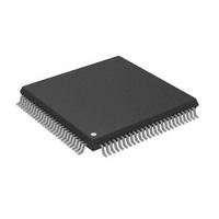
ADSP-2187LKSTZ-210 Analog Devices Inc, ADSP-2187LKSTZ-210 Datasheet - Page 8

ADSP-2187LKSTZ-210
Manufacturer Part Number
ADSP-2187LKSTZ-210
Description
IC DSP CONTRLR 16BIT 100-TQFP
Manufacturer
Analog Devices Inc
Series
ADSP-21xxr
Type
Fixed Pointr
Datasheet
1.ADSP-2184LBSTZ-160.pdf
(48 pages)
Specifications of ADSP-2187LKSTZ-210
Interface
Host Interface, Serial Port
Clock Rate
52MHz
Non-volatile Memory
External
On-chip Ram
160kB
Voltage - I/o
3.30V
Voltage - Core
3.30V
Operating Temperature
0°C ~ 70°C
Mounting Type
Surface Mount
Package / Case
100-TQFP, 100-VQFP
Device Core Size
16b
Format
Fixed Point
Clock Freq (max)
52.5MHz
Mips
52.5
Device Input Clock Speed
52.5MHz
Ram Size
160KB
Program Memory Size
Not RequiredKB
Operating Supply Voltage (typ)
3.3V
Operating Supply Voltage (min)
3V
Operating Supply Voltage (max)
3.6V
Operating Temp Range
0C to 70C
Operating Temperature Classification
Commercial
Mounting
Surface Mount
Pin Count
100
Package Type
LQFP
Lead Free Status / RoHS Status
Lead free / RoHS Compliant
Other names
ADSP-2187LKSTZ210
ADSP-2184L/ADSP-2185L/ADSP-2186L/ADSP-2187L
RESET
The RESET signal initiates a master reset of the ADSP-218xL.
The RESET signal must be asserted during the power-up
sequence to assure proper initialization. RESET during initial
power-up must be held long enough to allow the internal clock
to stabilize. If RESET is activated any time after power-up, the
clock continues to run and does not require stabilization time.
The power-up sequence is defined as the total time required for
the crystal oscillator circuit to stabilize after a valid V
applied to the processor, and for the internal phase-locked loop
(PLL) to lock onto the specific crystal frequency. A minimum of
2000 CLKIN cycles ensures that the PLL has locked, but does
not include the crystal oscillator start-up time. During this
power-up sequence, the RESET signal should be held low. On
any subsequent resets, the RESET signal must meet the mini-
mum pulse width specification (t
The RESET input contains some hysteresis; however, if an RC
circuit is used to generate the RESET signal, the use of an exter-
nal Schmitt trigger is recommended.
The master reset sets all internal stack pointers to the empty
stack condition, masks all interrupts, and clears the MSTAT
register. When RESET is released, if there is no pending bus
request and the chip is configured for booting, the boot-loading
Figure 3. External Crystal Connections
0x2000
0x3FFF
0x1FFF
0x0000
CLKIN
DSP
1M
PROGRAM MEMORY
EXTERNAL PM
XTAL
RESERVED
MODEB = 1
RSP
).
CLKOUT
Figure 4. ADSP-2184 Memory Architecture
Rev. C | Page 8 of 48 | January 2008
0x3FFF
0x1FFF
0x1000
0x0FFF
0x0000
0x2000
DD
is
PROGRAM MEMORY
PM OVERLAY 1,2
(EXTERNAL PM)
PM OVERLAY 0
INTERNAL PM
(RESERVED)
RESERVED
MODEB = 0
sequence is performed. The first instruction is fetched from on-
chip program memory location 0x0000 once boot loading
completes.
MEMORY ARCHITECTURE
The ADSP-218xL series provides a variety of memory and
peripheral interface options. The key functional groups are Pro-
gram Memory, Data Memory, Byte Memory, and I/O. Refer to
Figure 4
in the ADSP-218xL series.
Program Memory
Program Memory (Full Memory Mode) is a 24-bit-wide space
for storing both instruction opcodes and data. The member
DSPs of this series have up to 32K words of Program Memory
RAM on chip, and the capability of accessing up to two 8K
external memory overlay spaces, using the external data bus.
Program Memory (Host Mode) allows access to all internal
memory. External overlay access is limited by a single external
address line (A0). External program execution is not available in
Host Mode due to a restricted data bus that is only 16 bits wide.
Data Memory
Data Memory (Full Memory Mode) is a 16-bit-wide space used
for the storage of data variables and for memory-mapped con-
trol registers. The ADSP-218xL series has up to 32K words of
Data Memory RAM on-chip. Part of this space is used by 32
memory-mapped registers. Support also exists for up to two 8K
external memory overlay spaces through the external data bus.
All internal accesses complete in one cycle. Accesses to external
memory are timed using the wait states specified by the DWAIT
register.
Data Memory (Host Mode) allows access to all internal mem-
ory. External overlay access is limited by a single external
address line (A0).
through
0x2FFF
0x3FFF
0x3FE0
0x3FDF
0x3000
0x1FFF
0x2000
0x0000
Figure 7
CONTROL REGISTERS
32 MEMORY-MAPPED
DATA MEMORY
4064 RESERVED
DM OVERLAY 1,2
(EXTERNAL DM)
INTERNAL DM
DM OVERLAY 0
(RESERVED)
for PM and DM memory allocations
WORDS


