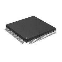
ADSP-2187LKSTZ-210 Analog Devices Inc, ADSP-2187LKSTZ-210 Datasheet - Page 21

ADSP-2187LKSTZ-210
Manufacturer Part Number
ADSP-2187LKSTZ-210
Description
IC DSP CONTRLR 16BIT 100-TQFP
Manufacturer
Analog Devices Inc
Series
ADSP-21xxr
Type
Fixed Pointr
Datasheet
1.ADSP-2184LBSTZ-160.pdf
(48 pages)
Specifications of ADSP-2187LKSTZ-210
Interface
Host Interface, Serial Port
Clock Rate
52MHz
Non-volatile Memory
External
On-chip Ram
160kB
Voltage - I/o
3.30V
Voltage - Core
3.30V
Operating Temperature
0°C ~ 70°C
Mounting Type
Surface Mount
Package / Case
100-TQFP, 100-VQFP
Device Core Size
16b
Format
Fixed Point
Clock Freq (max)
52.5MHz
Mips
52.5
Device Input Clock Speed
52.5MHz
Ram Size
160KB
Program Memory Size
Not RequiredKB
Operating Supply Voltage (typ)
3.3V
Operating Supply Voltage (min)
3V
Operating Supply Voltage (max)
3.6V
Operating Temp Range
0C to 70C
Operating Temperature Classification
Commercial
Mounting
Surface Mount
Pin Count
100
Package Type
LQFP
Lead Free Status / RoHS Status
Lead free / RoHS Compliant
Other names
ADSP-2187LKSTZ210
SPECIFICATIONS
OPERATING CONDITIONS
1
ELECTRICAL CHARACTERISTICS
1
2
3
4
5
6
7
8
9
Parameter
V
T
Specifications subject to change without notice.
Parameter
V
V
V
V
I
I
I
I
C
C
Specifications subject to change without notice.
Bidirectional pins: D23–0, RFS0, RFS1, SCLK0, SCLK1, TFS0, TFS1, A13–1, PF7–0.
Input only pins: CLKIN, RESET, BR, DR0, DR1, PWD.
Output pins: BG, PMS, DMS, BMS, IOMS, CMS, RD, WR, PWDACK, A0, DT0, DT1, CLKOUT, FL2–FL0, BGH.
Although specified for TTL outputs, all ADSP-218xL outputs are CMOS-compatible and will drive to V
Guaranteed but not tested.
Three-statable pins: A13–A1, D23–D0, PMS, DMS, BMS, IOMS, CMS, RD, WR, DT0, DT1, SCLK0, SCLK1, TFS0, TFS1, RFS0, RFS1, PF7–PF0.
0 V on BR.
Output pin capacitance is the capacitive load for any three-stated output pin.
IH
IL
OZH
OZL
AMB
DD
IH
IL
OH
OL
I
O
1
1
Description
Hi-Level Input Voltage
Lo-Level Input Voltage
Hi-Level Output Voltage
Lo-Level Output Voltage
Hi-Level Input Current
Lo-Level Input Current
Three-State Leakage Current
Three-State Leakage Current
Input Pin Capacitance
Output Pin Capacitance
3, 6
2, 3
3
2, 3
3
6, 7, 9
2, 4, 5
2, 4, 5
7
7
Min
3.0
0
Test Conditions
@ V
@ V
@ V
@ V
@ V
@ V
@ V
@ V
@ V
@ V
@ V
@ V
ADSP-2184L/ADSP-2185L/ADSP-2186L/ADSP-2187L
Rev. C | Page 21 of 48 | January 2008
DD
DD
DD
DD
DD
DD
DD
DD
DD
DD
IN
IN
= 3.5 V, f
= 2.5 V, f
= Max
= Max
= Min
= Min, I
= Min, I
= Min, I
= Max, V
= Max, V
= Max, V
= Max, V
K Grade (Commercial)
OH
OH
OL
IN
IN
IN
IN
IN
IN
= 1.0 MHz, T
= 1.0 MHz, T
= 2.0 mA
= –0.5 mA
= –100 μA
= V
= 0 V
= V
= 0 V
3.6
DD
DD
Max
+70
8
Max
Max
6
8
AMB
AMB
= 25°C
= 25°C
DD
and GND, assuming no dc loads.
Min
3.0
–40
Min
2.0
2.2
1.35
V
B Grade (Industrial)
DD
– 0.3
K and B Grades
3.6
Max
+85
Typ
Max
0.8
0.4
10
10
10
10
8
8
Unit
V
°C
Unit
V
V
V
V
V
V
μA
μA
μA
μA
pF
pF


