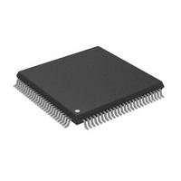
ADSP-2187LKSTZ-210 Analog Devices Inc, ADSP-2187LKSTZ-210 Datasheet - Page 3

ADSP-2187LKSTZ-210
Manufacturer Part Number
ADSP-2187LKSTZ-210
Description
IC DSP CONTRLR 16BIT 100-TQFP
Manufacturer
Analog Devices Inc
Series
ADSP-21xxr
Type
Fixed Pointr
Datasheet
1.ADSP-2184LBSTZ-160.pdf
(48 pages)
Specifications of ADSP-2187LKSTZ-210
Interface
Host Interface, Serial Port
Clock Rate
52MHz
Non-volatile Memory
External
On-chip Ram
160kB
Voltage - I/o
3.30V
Voltage - Core
3.30V
Operating Temperature
0°C ~ 70°C
Mounting Type
Surface Mount
Package / Case
100-TQFP, 100-VQFP
Device Core Size
16b
Format
Fixed Point
Clock Freq (max)
52.5MHz
Mips
52.5
Device Input Clock Speed
52.5MHz
Ram Size
160KB
Program Memory Size
Not RequiredKB
Operating Supply Voltage (typ)
3.3V
Operating Supply Voltage (min)
3V
Operating Supply Voltage (max)
3.6V
Operating Temp Range
0C to 70C
Operating Temperature Classification
Commercial
Mounting
Surface Mount
Pin Count
100
Package Type
LQFP
Lead Free Status / RoHS Status
Lead free / RoHS Compliant
Other names
ADSP-2187LKSTZ210
GENERAL DESCRIPTION
The ADSP-218xL series consists of four single chip microcom-
puters optimized for digital signal processing applications. The
functional block diagram for the ADSP-218xL series members
appears in
patible and are differentiated solely by the amount of on-chip
SRAM. This feature, combined with ADSP-21xx code compati-
bility, provides a great deal of flexibility in the design decision.
Specific family members are shown in
Table 1. ADSP-218xL DSP Microcomputer Family
ADSP-218xL series members combine the ADSP-2100 family
base architecture (three computational units, data address gen-
erators, and a program sequencer) with two serial ports, a 16-bit
internal DMA port, a byte DMA port, a programmable timer,
flag I/O, extensive interrupt capabilities, and on-chip program
and data memory.
ADSP-218xL series members integrate up to 160K bytes of on-
chip memory configured as up to 32K words (24-bit) of pro-
gram RAM, and up to 32K words (16-bit) of data RAM. Power-
down circuitry is also provided to meet the low power needs of
battery-operated portable equipment. The ADSP-218xL is avail-
able in 100-lead LQFP and 144-ball BGA packages.
Fabricated using high-speed, low-power, CMOS processes,
ADSP-218xL series members operate with a 19 ns instruction
cycle time (ADSP-2185L and ADSP-2187L) or a a 25 ns instruc-
tion cycle time (ADSP-2184L and ADSP-2186L). Every
instruction can execute in a single processor cycle.
The ADSP-218xL’s flexible architecture and comprehensive
instruction set allow the processor to perform multiple opera-
tions in parallel. In one processor cycle, ADSP-218xL series
members can:
This takes place while the processor continues to:
Device
ADSP-2184L
ADSP-2185L
ADSP-2186L
ADSP-2187L
• Generate the next program address
• Fetch the next instruction
• Perform one or two data moves
• Update one or two data address pointers
• Perform a computational operation
• Receive and transmit data through the two serial ports
• Receive and/or transmit data through the internal
• Receive and/or transmit data through the byte DMA port
• Decrement timer
DMA port
Figure 1 on Page
Program Memory
(K words)
4
16
8
32
1. All series members are pin-com-
Table
Data Memory
(K words)
4
16
8
32
1.
ADSP-2184L/ADSP-2185L/ADSP-2186L/ADSP-2187L
Rev. C | Page 3 of 48 | January 2008
ARCHITECTURE OVERVIEW
The ADSP-218xL series instruction set provides flexible data
moves and multifunction (one or two data moves with a com-
putation) instructions. Every instruction can be executed in a
single processor cycle. The ADSP-218xL assembly language uses
an algebraic syntax for ease of coding and readability. A com-
prehensive set of development tools supports program
development.
The functional block diagram is an overall block diagram of the
ADSP-218xL series. The processor contains three independent
computational units: the ALU, the multiplier/accumulator
(MAC), and the shifter. The computational units process 16-bit
data directly and have provisions to support multiprecision
computations. The ALU performs a standard set of arithmetic
and logic operations; division primitives are also supported. The
MAC performs single-cycle multiply, multiply/add, and multi-
ply/subtract operations with 40 bits of accumulation. The shifter
performs logical and arithmetic shifts, normalization, denor-
malization, and derive exponent operations.
The shifter can be used to efficiently implement numeric format
control, including multiword and block floating-point
representations.
The internal result (R) bus connects the computational units so
that the output of any unit may be the input of any unit on the
next cycle.
A powerful program sequencer and two dedicated data address
generators ensure efficient delivery of operands to these compu-
tational units. The sequencer supports conditional jumps,
subroutine calls, and returns in a single cycle. With internal
loop counters and loop stacks, ADSP-218xL series members
execute looped code with zero overhead; no explicit jump
instructions are required to maintain loops.
Two data address generators (DAGs) provide addresses for
simultaneous dual operand fetches (from data memory and pro-
gram memory). Each DAG maintains and updates four address
pointers. Whenever the pointer is used to access data (indirect
addressing), it is post-modified by the value of one of four possi-
ble modify registers. A length value may be associated with each
pointer to implement automatic modulo addressing for
circular buffers.
Five internal buses provide efficient data transfer:
• Program Memory Address (PMA) Bus
• Program Memory Data (PMD) Bus
• Data Memory Address (DMA) Bus
• Data Memory Data (DMD) Bus
• Result (R) Bus


