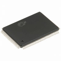
CY7C68013A-128AXI Cypress Semiconductor Corp, CY7C68013A-128AXI Datasheet - Page 11

CY7C68013A-128AXI
Manufacturer Part Number
CY7C68013A-128AXI
Description
IC MCU USB PERIPH HI SPD 128LQFP
Manufacturer
Cypress Semiconductor Corp
Series
EZ-USB FX2LP™r
Specifications of CY7C68013A-128AXI
Program Memory Type
ROMless
Package / Case
128-LQFP
Applications
USB Microcontroller
Core Processor
8051
Controller Series
CY7C680xx
Ram Size
16K x 8
Interface
I²C, USB, USART
Number Of I /o
40
Voltage - Supply
3 V ~ 3.6 V
Operating Temperature
-40°C ~ 85°C
Mounting Type
Surface Mount
Processor Series
CY7C68xx
Core
8051
Data Bus Width
8 bit
Data Ram Size
16 KB
Interface Type
I2C, USART, USB
Maximum Clock Frequency
48 MHz
Number Of Programmable I/os
40
Number Of Timers
3
Maximum Operating Temperature
+ 105 C
Mounting Style
SMD/SMT
Development Tools By Supplier
CY3684
Minimum Operating Temperature
- 40 C
Controller Family/series
(8051) USB
Core Size
8 Bit
No. Of I/o's
40
Program Memory Size
16KB
Cpu Speed
48MHz
No. Of Timers
3
Embedded Interface Type
I2C, USART, USB
Rohs Compliant
Yes
Lead Free Status / RoHS Status
Lead free / RoHS Compliant
For Use With
CY4611B - KIT USB TO ATA REFERENCE DESIGN428-1677 - KIT DEVELOPMENT EZ-USB FX2LP
Lead Free Status / Rohs Status
Lead free / RoHS Compliant
Other names
428-1943
CY7C68013A-128AXI
CY7C68013A-128AXI
Available stocks
Company
Part Number
Manufacturer
Quantity
Price
Company:
Part Number:
CY7C68013A-128AXI
Manufacturer:
EPCOS
Quantity:
43 000
Company:
Part Number:
CY7C68013A-128AXI
Manufacturer:
CY
Quantity:
5 530
Company:
Part Number:
CY7C68013A-128AXI
Manufacturer:
CY
Quantity:
6 100
Company:
Part Number:
CY7C68013A-128AXI
Manufacturer:
Cypress Semiconductor Corp
Quantity:
10 000
3.12.5 Default Full Speed Alternate Settings
Table 6. Default Full Speed Alternate Settings
3.12.6 Default High Speed Alternate Settings
Table 7. Default High Speed Alternate Settings
3.13 External FIFO Interface
3.13.1 Architecture
The FX2LP slave FIFO architecture has eight 512 byte blocks in
the endpoint RAM that directly serve as FIFO memories and are
controlled by FIFO control signals (such as IFCLK, SLCS#,
SLRD, SLWR, SLOE, PKTEND, and flags).
In operation, some of the eight RAM blocks fill or empty from the
SIE, while the others are connected to the I/O transfer logic. The
transfer logic takes two forms, the GPIF for internally generated
control signals and the slave FIFO interface for externally
controlled transfers.
3.13.2 Master/Slave Control Signals
The FX2LP endpoint FIFOS are implemented as eight physically
distinct 256x16 RAM blocks. The 8051/SIE can switch any of the
RAM blocks between two domains, the USB (SIE) domain and
the 8051-I/O Unit domain. This switching is done virtually instan-
taneously, giving essentially zero transfer time between “USB
FIFOS” and “Slave FIFOS.” Because they are physically the
same memory no bytes are actually transferred between buffers.
At any given time, some RAM blocks are filling/emptying with
USB data under SIE control, while other RAM blocks are
available to the 8051, the I/O control unit or both. The RAM
blocks operate as single port in the USB domain, and dual port
Document #: 38-08032 Rev. *M
Notes
ep0
ep1out
ep1in
ep2
ep4
ep6
ep8
ep0
ep1out
ep1in
ep2
ep4
ep6
ep8
4. “0” means “not implemented.”
5. “2×” means “double buffered.”
6. Even though these buffers are 64 bytes, they are reported as 512 for USB 2.0 compliance. The user must never transfer packets larger than 64 bytes to EP1.
Alternate Setting
Alternate Setting
64
0
0
0
0
0
0
0
64
0
0
0
0
0
0
0
64
512 bulk
512 bulk
512 bulk out (2×)
512 bulk out (2×)
512 bulk in (2×)
512 bulk in (2×)
64
64 bulk
64 bulk
64 bulk out (2×)
64 bulk out (2×)
64 bulk in (2×)
64 bulk in (2×)
[6]
[6]
[4, 5]
[4, 5]
1
1
in the 8051-I/O domain. The blocks can be configured as single,
double, triple, or quad buffered as previously shown.
The I/O control unit implements either an internal master (M for
master) or external master (S for Slave) interface.
In Master (M) mode, the GPIF internally controls FIFOADR[1..0]
to select a FIFO. The RDY pins (two in the 56-pin package, six
in the 100-pin and 128-pin packages) can be used as flag inputs
from an external FIFO or other logic if desired. The GPIF can be
run from either an internally derived clock or externally supplied
clock (IFCLK), at a rate that transfers data up to 96 Megabytes/s
(48-MHz IFCLK with 16-bit interface).
In Slave (S) mode, the FX2LP accepts either an internally
derived clock or externally supplied clock (IFCLK, max frequency
48 MHz) and SLCS#, SLRD, SLWR, SLOE, PKTEND signals
from external logic. When using an external IFCLK, the external
clock must be present before switching to the external clock with
the IFCLKSRC bit. Each endpoint can individually be selected
for byte or word operation by an internal configuration bit and a
Slave FIFO Output Enable signal SLOE enables data of the
selected width. External logic must ensure that the output enable
signal is inactive when writing data to a slave FIFO. The slave
interface can also operate asynchronously, where the SLRD and
SLWR signals act directly as strobes, rather than a clock qualifier
as in synchronous mode. The signals SLRD, SLWR, SLOE and
PKTEND are gated by the signal SLCS#.
64
64 int
64 int
512 int out (2×)
512 bulk out (2×)
512 int in (2×)
512 bulk in (2×)
64
64 int
64 int
64 int out (2×)
64 bulk out (2×)
64 int in (2×)
64 bulk in (2×)
2
2
CY7C68013A, CY7C68014A
CY7C68015A, CY7C68016A
64
64 int
64 int
512 iso out (2×)
512 bulk out (2×)
512 iso in (2×)
512 bulk in (2×)
64
64 int
64 int
64 iso out (2×)
64 bulk out (2×)
64 iso in (2×)
64 bulk in (2×)
3
3
Page 11 of 62
[+] Feedback


