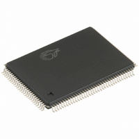
CY7C68013A-128AXI Cypress Semiconductor Corp, CY7C68013A-128AXI Datasheet - Page 53

CY7C68013A-128AXI
Manufacturer Part Number
CY7C68013A-128AXI
Description
IC MCU USB PERIPH HI SPD 128LQFP
Manufacturer
Cypress Semiconductor Corp
Series
EZ-USB FX2LP™r
Specifications of CY7C68013A-128AXI
Program Memory Type
ROMless
Package / Case
128-LQFP
Applications
USB Microcontroller
Core Processor
8051
Controller Series
CY7C680xx
Ram Size
16K x 8
Interface
I²C, USB, USART
Number Of I /o
40
Voltage - Supply
3 V ~ 3.6 V
Operating Temperature
-40°C ~ 85°C
Mounting Type
Surface Mount
Processor Series
CY7C68xx
Core
8051
Data Bus Width
8 bit
Data Ram Size
16 KB
Interface Type
I2C, USART, USB
Maximum Clock Frequency
48 MHz
Number Of Programmable I/os
40
Number Of Timers
3
Maximum Operating Temperature
+ 105 C
Mounting Style
SMD/SMT
Development Tools By Supplier
CY3684
Minimum Operating Temperature
- 40 C
Controller Family/series
(8051) USB
Core Size
8 Bit
No. Of I/o's
40
Program Memory Size
16KB
Cpu Speed
48MHz
No. Of Timers
3
Embedded Interface Type
I2C, USART, USB
Rohs Compliant
Yes
Lead Free Status / RoHS Status
Lead free / RoHS Compliant
For Use With
CY4611B - KIT USB TO ATA REFERENCE DESIGN428-1677 - KIT DEVELOPMENT EZ-USB FX2LP
Lead Free Status / Rohs Status
Lead free / RoHS Compliant
Other names
428-1943
CY7C68013A-128AXI
CY7C68013A-128AXI
Available stocks
Company
Part Number
Manufacturer
Quantity
Price
Company:
Part Number:
CY7C68013A-128AXI
Manufacturer:
EPCOS
Quantity:
43 000
Company:
Part Number:
CY7C68013A-128AXI
Manufacturer:
CY
Quantity:
5 530
Company:
Part Number:
CY7C68013A-128AXI
Manufacturer:
CY
Quantity:
6 100
Company:
Part Number:
CY7C68013A-128AXI
Manufacturer:
Cypress Semiconductor Corp
Quantity:
10 000
10.17.4 Sequence Diagram of a Single and Burst Asynchronous Write
Figure 34
in an asynchronous mode. The diagram shows a single write
followed by a burst write of 3 bytes and committing the 4 byte
short packet using PKTEND.
■
■
■
■
Document #: 38-08032 Rev. *M
At t = 0 the FIFO address is applied, insuring that it meets the
setup time of t
(SLCS may be tied low in some applications).
At t = 1 SLWR is asserted. SLWR must meet the minimum
active pulse of t
t
before SLWR is asserted.
At t = 2, data must be present on the bus t
deasserting edge of SLWR.
At t = 3, deasserting SLWR causes the data to be written from
the data bus to the FIFO and then increments the FIFO pointer.
WRpwh
FIFOADR
PKTEND
FLAGS
SLWR
DATA
SLCS
. If the SLCS is used, it must be asserted with SLWR or
shows the timing relationship of the SLAVE FIFO write
t=0
SFA
WRpwl
t
SFA
. If SLCS is used, it must also be asserted
t =1
Figure 34. Slave FIFO Asynchronous Write Sequence and Timing Diagram
t
and minimum de-active pulse width of
WRpwl
t=2
t
SFD
t=3
N
t
t
FDH
WRpwh
t
FAH
t
XFLG
SFD
T=0
t
before the
SFA
T=1
t
WRpwl
T=2
t
SFD
T=3
t
N+1
FDH
t
WRpwh
T=4
The same sequence of events are shown for a burst write and is
indicated by the timing marks of T = 0 through 5.
Note In the burst write mode, after SLWR is deasserted, the data
is written to the FIFO and then the FIFO pointer is incremented
to the next byte in the FIFO. The FIFO pointer is post incre-
mented.
In
SLWR is deasserted, the short 4 byte packet can be committed
to the host using the PKTEND. The external device should be
designed to not assert SLWR and the PKTEND signal at the
same time. It should be designed to assert the PKTEND after
SLWR is deasserted and met the minimum deasserted pulse
width. The FIFOADDR lines have to held constant during the
PKTEND assertion.
t
WRpwl
T=5
The FIFO flag is also updated after t
edge of SLWR.
Figure 34
t
SFD
T=6
t
N+2
FDH
t
WRpwh
after the four bytes are written to the FIFO and
T=7
t
WRpwl
CY7C68013A, CY7C68014A
CY7C68015A, CY7C68016A
T=8
t
SFD
T=9
t
t
N+3
WRpwh
FDH
[20]
t
XFLG
PEpwl
from the deasserting
t
XFLG
t
Page 53 of 62
PEpwh
t
FAH
[+] Feedback


