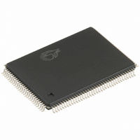
CY7C68013A-128AXI Cypress Semiconductor Corp, CY7C68013A-128AXI Datasheet - Page 14

CY7C68013A-128AXI
Manufacturer Part Number
CY7C68013A-128AXI
Description
IC MCU USB PERIPH HI SPD 128LQFP
Manufacturer
Cypress Semiconductor Corp
Series
EZ-USB FX2LP™r
Specifications of CY7C68013A-128AXI
Program Memory Type
ROMless
Package / Case
128-LQFP
Applications
USB Microcontroller
Core Processor
8051
Controller Series
CY7C680xx
Ram Size
16K x 8
Interface
I²C, USB, USART
Number Of I /o
40
Voltage - Supply
3 V ~ 3.6 V
Operating Temperature
-40°C ~ 85°C
Mounting Type
Surface Mount
Processor Series
CY7C68xx
Core
8051
Data Bus Width
8 bit
Data Ram Size
16 KB
Interface Type
I2C, USART, USB
Maximum Clock Frequency
48 MHz
Number Of Programmable I/os
40
Number Of Timers
3
Maximum Operating Temperature
+ 105 C
Mounting Style
SMD/SMT
Development Tools By Supplier
CY3684
Minimum Operating Temperature
- 40 C
Controller Family/series
(8051) USB
Core Size
8 Bit
No. Of I/o's
40
Program Memory Size
16KB
Cpu Speed
48MHz
No. Of Timers
3
Embedded Interface Type
I2C, USART, USB
Rohs Compliant
Yes
Lead Free Status / RoHS Status
Lead free / RoHS Compliant
For Use With
CY4611B - KIT USB TO ATA REFERENCE DESIGN428-1677 - KIT DEVELOPMENT EZ-USB FX2LP
Lead Free Status / Rohs Status
Lead free / RoHS Compliant
Other names
428-1943
CY7C68013A-128AXI
CY7C68013A-128AXI
Available stocks
Company
Part Number
Manufacturer
Quantity
Price
Company:
Part Number:
CY7C68013A-128AXI
Manufacturer:
EPCOS
Quantity:
43 000
Company:
Part Number:
CY7C68013A-128AXI
Manufacturer:
CY
Quantity:
5 530
Company:
Part Number:
CY7C68013A-128AXI
Manufacturer:
CY
Quantity:
6 100
Company:
Part Number:
CY7C68013A-128AXI
Manufacturer:
Cypress Semiconductor Corp
Quantity:
10 000
3.20 CY7C68013A/14A and CY7C68015A/16A
CY7C68013A is identical to CY7C68014A in form, fit, and
functionality. CY7C68015A is identical to CY7C68016A in form,
fit, and functionality. CY7C68014A and CY7C68016A have a
lower suspend current than CY7C68013A and CY7C68015A
respectively and are ideal for power sensitive battery applica-
tions.
CY7C68015A and CY7C68016A are available in 56-pin QFN
package only. Two additional GPIO signals are available on the
CY7C68015A and CY7C68016A to provide more flexibility when
neither IFCLK or CLKOUT are needed in the 56-pin package.
USB developers wanting to convert their FX2 56-pin application
to a bus-powered system directly benefit from these additional
signals. The two GPIOs give developers the signals they need
for the power control circuitry of their bus-powered application
without pushing them to a high pincount version of FX2LP.
The CY7C68015A is only available in the 56-pin QFN package
Table 10. CY7C68013A/14A and CY7C68015A/16A Pin Dif-
ferences
Document #: 38-08032 Rev. *M
CY7C68013A/CY7C68014A CY7C68015A/CY7C68016A
Differences
CLKOUT
IFCLK
PE0
PE1
4. Pin Assignments
Figure 6
types. The following pages illustrate the individual pin diagrams,
plus a combination diagram showing which of the full set of
signals are available in the 128-pin, 100-pin, and 56-pin
packages.
The signals on the left edge of the 56-pin package in
on page 15 are common to all versions in the FX2LP family with
the noted differences between the CY7C68013A/14A and the
CY7C68015A/16A.
Three modes are available in all package versions: Port, GPIF
master, and Slave FIFO. These modes define the signals on the
right edge of the diagram. The 8051 selects the interface mode
using the IFCONFIG[1:0] register bits. Port mode is the power on
default configuration.
The 100-pin package adds functionality to the 56-pin package by
adding these pins:
■
■
■
■
■
■
The 128-pin package adds the 8051 address and data buses
plus control signals. Note that two of the required signals, RD#
and WR#, are present in the 100-pin version.
In the 100-pin and 128-pin versions, an 8051 control bit can be
set to pulse the RD# and WR# pins when the 8051 reads
from/writes to PORTC. This feature is enabled by setting
PORTCSTB bit in CPUCS register.
Section 10.5
strobing function on accessing PORTC.
PORTC or alternate GPIFADR[7:0] address signals
PORTE or alternate GPIFADR[8] address signal and seven
additional 8051 signals
Three GPIF Control signals
Four GPIF Ready signals
Nine 8051 signals (two USARTs, three timer inputs, INT4,and
INT5#)
BKPT, RD#, WR#.
on page 15 identifies all signals for the five package
displays the timing diagram of the read and write
CY7C68013A, CY7C68014A
CY7C68015A, CY7C68016A
Page 14 of 62
Figure 6
[+] Feedback


