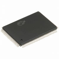
CY7C68013A-128AXI Cypress Semiconductor Corp, CY7C68013A-128AXI Datasheet - Page 41

CY7C68013A-128AXI
Manufacturer Part Number
CY7C68013A-128AXI
Description
IC MCU USB PERIPH HI SPD 128LQFP
Manufacturer
Cypress Semiconductor Corp
Series
EZ-USB FX2LP™r
Specifications of CY7C68013A-128AXI
Program Memory Type
ROMless
Package / Case
128-LQFP
Applications
USB Microcontroller
Core Processor
8051
Controller Series
CY7C680xx
Ram Size
16K x 8
Interface
I²C, USB, USART
Number Of I /o
40
Voltage - Supply
3 V ~ 3.6 V
Operating Temperature
-40°C ~ 85°C
Mounting Type
Surface Mount
Processor Series
CY7C68xx
Core
8051
Data Bus Width
8 bit
Data Ram Size
16 KB
Interface Type
I2C, USART, USB
Maximum Clock Frequency
48 MHz
Number Of Programmable I/os
40
Number Of Timers
3
Maximum Operating Temperature
+ 105 C
Mounting Style
SMD/SMT
Development Tools By Supplier
CY3684
Minimum Operating Temperature
- 40 C
Controller Family/series
(8051) USB
Core Size
8 Bit
No. Of I/o's
40
Program Memory Size
16KB
Cpu Speed
48MHz
No. Of Timers
3
Embedded Interface Type
I2C, USART, USB
Rohs Compliant
Yes
Lead Free Status / RoHS Status
Lead free / RoHS Compliant
For Use With
CY4611B - KIT USB TO ATA REFERENCE DESIGN428-1677 - KIT DEVELOPMENT EZ-USB FX2LP
Lead Free Status / Rohs Status
Lead free / RoHS Compliant
Other names
428-1943
CY7C68013A-128AXI
CY7C68013A-128AXI
Available stocks
Company
Part Number
Manufacturer
Quantity
Price
Company:
Part Number:
CY7C68013A-128AXI
Manufacturer:
EPCOS
Quantity:
43 000
Company:
Part Number:
CY7C68013A-128AXI
Manufacturer:
CY
Quantity:
5 530
Company:
Part Number:
CY7C68013A-128AXI
Manufacturer:
CY
Quantity:
6 100
Company:
Part Number:
CY7C68013A-128AXI
Manufacturer:
Cypress Semiconductor Corp
Quantity:
10 000
10.5 PORTC Strobe Feature Timings
The RD# and WR# are present in the 100-pin version and the
128-pin package. In these 100-pin and 128-pin versions, an
8051 control bit can be set to pulse the RD# and WR# pins when
the 8051 reads from or writes to PORTC. This feature is enabled
by setting PORTCSTB bit in CPUCS register.
The RD# and WR# strobes are asserted for two CLKOUT cycles
when PORTC is accessed.
The WR# strobe is asserted two clock cycles after PORTC is
updated and is active for two clock cycles after that, as shown in
Figure
As for read, the value of PORTC three clock cycles before the
assertion of RD# is the value that the 8051 reads in. The RD# is
pulsed for 2 clock cycles after 3 clock cycles from the point when
the 8051 has performed a read function on PORTC.
Document #: 38-08032 Rev. *M
PORTC IS UPDATED
CLKOUT
WR#
CLKOUT
8051 READS PORTC
RD#
15.
Figure 15. WR# Strobe Function when PORTC is Accessed by 8051
Figure 16. RD# Strobe Function when PORTC is Accessed by 8051
t
t
CLKOUT
CLKOUT
DATA MUST BE HELD FOR 3 CLK CYLCES
t
The RD# signal prompts the external logic to prepare the next
data byte. Nothing gets sampled internally on assertion of the
RD# signal itself, it is just a prefetch type signal to get the next
data byte prepared. So, using it with that in mind easily meets the
setup time to the next read.
The purpose of this pulsing of RD# is to allow the external
peripheral to know that the 8051 is done reading PORTC and the
data was latched into PORTC three CLKOUT cycles before
asserting the RD# signal. After the RD# is pulsed, the external
logic can update the data on PORTC.
Following is the timing diagram of the read and write strobing
function on accessing PORTC. Refer to
Section 10.4
signals.
STBL
t
for details on propagation delay of RD# and WR#
STBL
DATA CAN BE UPDATED BY EXTERNAL LOGIC
CY7C68013A, CY7C68014A
CY7C68015A, CY7C68016A
t
STBH
t
STBH
Page 41 of 62
Section 10.3
and
[+] Feedback


