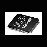
LPC2361_62 NXP Semiconductors, LPC2361_62 Datasheet - Page 19

LPC2361_62
Manufacturer Part Number
LPC2361_62
Description
The LPC2361/2362 microcontrollers are based on a 16-bit/32-bit ARM7TDMI-S CPU with real-time emulation that combines the microcontroller with up to 128 kB of embedded high-speed flash memory
Manufacturer
NXP Semiconductors
Datasheet
1.LPC2361_62.pdf
(64 pages)
NXP Semiconductors
LPC2361_62
Product data sheet
7.10.1.1 Features
7.10.1 USB device controller
7.10 USB interface
The Universal Serial Bus (USB) is a 4-wire bus that supports communication between a
host and one or more (up to 127) peripherals. The Host Controller allocates the USB
bandwidth to attached devices through a token-based protocol. The bus supports hot
plugging and dynamic configuration of the devices. All transactions are initiated by the
Host Controller.
The LPC2361/2362 USB interface includes a device, Host, and OTG Controller. Details
on typical USB interfacing solutions can be found in
The device controller enables 12 Mbit/s data exchange with a USB Host Controller. It
consists of a register interface, serial interface engine, endpoint buffer memory, and a
DMA controller. The serial interface engine decodes the USB data stream and writes data
to the appropriate endpoint buffer. The status of a completed USB transfer or error
condition is indicated via status registers. An interrupt is also generated if enabled. When
enabled, the DMA controller transfers data between the endpoint buffer and the USB
RAM.
•
•
•
•
•
•
Memory management:
– Independent transmit and receive buffers memory mapped to shared SRAM.
– DMA managers with scatter/gather DMA and arrays of frame descriptors.
– Memory traffic optimized by buffering and pre-fetching.
Enhanced Ethernet features:
– Receive filtering.
– Multicast and broadcast frame support for both transmit and receive.
– Optional automatic Frame Check Sequence (FCS) insertion with Circular
– Selectable automatic transmit frame padding.
– Over-length frame support for both transmit and receive allows any length frames.
– Promiscuous receive mode.
– Automatic collision back-off and frame retransmission.
– Includes power management by clock switching.
– Wake-on-LAN power management support allows system wake-up: using the
Physical interface:
– Attachment of external PHY chip through standard RMII interface.
– PHY register access is available via the MIIM interface.
Fully compliant with USB 2.0 specification (full speed).
Supports 32 physical (16 logical) endpoints with a 4 kB endpoint buffer RAM.
Supports Control, Bulk, Interrupt and Isochronous endpoints.
Redundancy Check (CRC) for transmit.
receive filters or a magic frame detection filter.
All information provided in this document is subject to legal disclaimers.
Rev. 5 — 25 October 2011
Section
Single-chip 16-bit/32-bit MCU
14.1.
LPC2361/62
© NXP B.V. 2011. All rights reserved.
19 of 64


