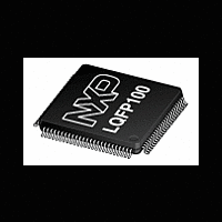
LPC2361_62 NXP Semiconductors, LPC2361_62 Datasheet - Page 30

LPC2361_62
Manufacturer Part Number
LPC2361_62
Description
The LPC2361/2362 microcontrollers are based on a 16-bit/32-bit ARM7TDMI-S CPU with real-time emulation that combines the microcontroller with up to 128 kB of embedded high-speed flash memory
Manufacturer
NXP Semiconductors
Datasheet
1.LPC2361_62.pdf
(64 pages)
NXP Semiconductors
LPC2361_62
Product data sheet
7.23.4.5 Power domains
7.24.1 Reset
7.24 System control
While in Deep power-down mode, external device power may be removed. In this case,
the LPC2361/2362 will start up when external power is restored.
Essential data may be retained through Deep power-down mode (or through complete
powering off of the chip) by storing data in the Battery RAM, as long as the external power
to the VBAT pin is maintained.
The LPC2361/2362 provides two independent power domains that allow the bulk of the
device to have power removed while maintaining operation of the RTC and the battery
RAM.
On the LPC2361/2362, I/O pads are powered by the 3.3 V (V
V
the CPU and most of the peripherals.
Depending on the LPC2361/2362 application, a design can use two power options to
manage power consumption.
The first option assumes that power consumption is not a concern and the design ties the
V
supply for both pads, the CPU, and peripherals. While this solution is simple, it does not
support powering down the I/O pad ring “on the fly” while keeping the CPU and
peripherals alive.
The second option uses two power supplies; a 3.3 V supply for the I/O pads (V
a dedicated 3.3 V supply for the CPU (V
converter powered independently from the I/O pad ring enables shutting down of the I/O
pad power supply “on the fly”, while the CPU and peripherals stay active.
The VBAT pin supplies power only to the RTC and the battery RAM. These two functions
require a minimum of power to operate, which can be supplied by an external battery.
When the CPU and the rest of chip functions are stopped and power removed, the RTC
can supply an alarm output that may be used by external hardware to restore chip power
and resume operation.
Reset has four sources on the LPC2361/2362: the RESET pin, the watchdog reset,
power-on reset, and the BrownOut Detection (BOD) circuit. The RESET pin is a Schmitt
trigger input pin. Assertion of chip Reset by any source, once the operating voltage attains
a usable level, starts the wake-up timer (see description in
timer”), causing reset to remain asserted until the external Reset is de-asserted, the
oscillator is running, a fixed number of clocks have passed, and the flash controller has
completed its initialization.
When the internal Reset is removed, the processor begins executing at address 0, which
is initially the Reset vector mapped from the Boot Block. At that point, all of the processor
and peripheral registers have been initialized to predetermined values.
DD(DCDC)(3V3)
DD(3V3)
and V
pin powers the on-chip DC-to-DC converter which in turn provides power to
DD(DCDC)(3V3)
All information provided in this document is subject to legal disclaimers.
Rev. 5 — 25 October 2011
pins together. This approach requires only one 3.3 V power
DD(DCDC)(3V3)
). Having the on-chip DC-to-DC
Single-chip 16-bit/32-bit MCU
Section 7.23.3 “Wake-up
DD(3V3)
LPC2361/62
) pins, while the
© NXP B.V. 2011. All rights reserved.
DD(3V3)
30 of 64
) and


