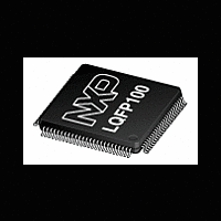
LPC2367FBD100 NXP Semiconductors, LPC2367FBD100 Datasheet - Page 13

LPC2367FBD100
Manufacturer Part Number
LPC2367FBD100
Description
The LPC2367FBD100 is a ARM7 microcontroller for embedded applications featuring a high level of integration and low power consumption at frequencies of 72 MHz
Manufacturer
NXP Semiconductors
Datasheet
1.LPC2364FET100.pdf
(69 pages)
Available stocks
Company
Part Number
Manufacturer
Quantity
Price
Company:
Part Number:
LPC2367FBD100
Manufacturer:
TI
Quantity:
160
Part Number:
LPC2367FBD100
Manufacturer:
ST
Quantity:
20 000
Company:
Part Number:
LPC2367FBD100,551
Manufacturer:
NXP Semiconductors
Quantity:
10 000
NXP Semiconductors
Table 4.
LPC2364_65_66_67_68
Product data sheet
Symbol
P1[0]/
ENET_TXD0
P1[1]/
ENET_TXD1
P1[4]/
ENET_TX_EN
P1[8]/
ENET_CRS
P1[9]/
ENET_RXD0
P1[10]/
ENET_RXD1
P1[14]/
ENET_RX_ER
P1[15]/
ENET_REF_CLK
P1[16]/
ENET_MDC
P1[17]/
ENET_MDIO
P1[18]/
USB_UP_LED/
PWM1[1]/
CAP1[0]
P1[19]/CAP1[1]
P1[20]/PWM1[2]/
SCK0
P1[21]/PWM1[3]/
SSEL0
P1[22]/MAT1[0]
Pin description
Pin
95
94
93
92
91
90
89
88
87
86
32
33
34
35
36
[1]
[1]
[1]
[1]
[1]
[1]
[1]
[1]
[1]
[1]
[1]
[1]
[1]
[1]
[1]
…continued
Ball
D5
B4
A4
C5
B5
A5
D6
C6
A6
B6
H4
J4
K4
F5
J5
[1]
[1]
[1]
[1]
[1]
[1]
[1]
[1]
[1]
[1]
[1]
[1]
[1]
[1]
[1]
Type
I/O
O
I/O
O
I/O
O
I/O
I
I/O
I
I/O
I
I/O
I
I/O
I
I/O
O
I/O
I/O
I/O
O
O
I
I/O
I
I/O
O
I/O
I/O
O
I/O
I/O
O
All information provided in this document is subject to legal disclaimers.
Description
P1[0] — General purpose digital input/output pin.
ENET_TXD0 — Ethernet transmit data 0.
P1[1] — General purpose digital input/output pin.
ENET_TXD1 — Ethernet transmit data 1.
P1[4] — General purpose digital input/output pin.
ENET_TX_EN — Ethernet transmit data enable.
P1[8] — General purpose digital input/output pin.
ENET_CRS — Ethernet carrier sense.
P1[9] — General purpose digital input/output pin.
ENET_RXD0 — Ethernet receive data.
P1[10] — General purpose digital input/output pin.
ENET_RXD1 — Ethernet receive data.
P1[14] — General purpose digital input/output pin.
ENET_RX_ER — Ethernet receive error.
P1[15] — General purpose digital input/output pin.
ENET_REF_CLK — Ethernet reference clock.
P1[16] — General purpose digital input/output pin.
ENET_MDC — Ethernet MIIM clock.
P1[17] — General purpose digital input/output pin.
ENET_MDIO — Ethernet MIIM data input and output.
P1[18] — General purpose digital input/output pin.
USB_UP_LED — USB GoodLink LED indicator. It is LOW when device is
configured (non-control endpoints enabled), or when host is enabled and
has detected a device on the bus. It is HIGH when the device is not
configured, or when host is enabled and has not detected a device on the
bus, or during global suspend. It transitions between LOW and HIGH
(flashes) when host is enabled and detects activity on the bus.
(LPC2364/66/68 only)
PWM1[1] — Pulse Width Modulator 1, channel 1 output.
CAP1[0] — Capture input for Timer 1, channel 0.
P1[19] — General purpose digital input/output pin.
CAP1[1] — Capture input for Timer 1, channel 1.
P1[20] — General purpose digital input/output pin.
PWM1[2] — Pulse Width Modulator 1, channel 2 output.
SCK0 — Serial clock for SSP0.
P1[21] — General purpose digital input/output pin.
PWM1[3] — Pulse Width Modulator 1, channel 3 output.
SSEL0 — Slave Select for SSP0.
P1[22] — General purpose digital input/output pin.
MAT1[0] — Match output for Timer 1, channel 0.
Rev. 7 — 20 October 2011
LPC2364/65/66/67/68
Single-chip 16-bit/32-bit microcontrollers
© NXP B.V. 2011. All rights reserved.
13 of 69


