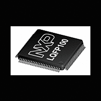
LPC2367FBD100 NXP Semiconductors, LPC2367FBD100 Datasheet - Page 21

LPC2367FBD100
Manufacturer Part Number
LPC2367FBD100
Description
The LPC2367FBD100 is a ARM7 microcontroller for embedded applications featuring a high level of integration and low power consumption at frequencies of 72 MHz
Manufacturer
NXP Semiconductors
Datasheet
1.LPC2364FET100.pdf
(69 pages)
Available stocks
Company
Part Number
Manufacturer
Quantity
Price
Company:
Part Number:
LPC2367FBD100
Manufacturer:
TI
Quantity:
160
Part Number:
LPC2367FBD100
Manufacturer:
ST
Quantity:
20 000
Company:
Part Number:
LPC2367FBD100,551
Manufacturer:
NXP Semiconductors
Quantity:
10 000
NXP Semiconductors
LPC2364_65_66_67_68
Product data sheet
7.5.1 Interrupt sources
7.7.1 Features
7.6 Pin connect block
7.7 General purpose DMA controller
FIQs have the highest priority. If more than one request is assigned to FIQ, the VIC ORs
the requests to produce the FIQ signal to the ARM processor. The fastest possible FIQ
latency is achieved when only one request is classified as FIQ, because then the FIQ
service routine can simply start dealing with that device. But if more than one request is
assigned to the FIQ class, the FIQ service routine can read a word from the VIC that
identifies which FIQ source(s) is (are) requesting an interrupt.
Vectored IRQs, which include all interrupt requests that are not classified as FIQs, have a
programmable interrupt priority. When more than one interrupt is assigned the same
priority and occur simultaneously, the one connected to the lowest numbered VIC channel
will be serviced first.
The VIC ORs the requests from all of the vectored IRQs to produce the IRQ signal to the
ARM processor. The IRQ service routine can start by reading a register from the VIC and
jumping to the address supplied by that register.
Each peripheral device has one interrupt line connected to the VIC but may have several
interrupt flags. Individual interrupt flags may also represent more than one interrupt
source.
Any pin on Port 0 and Port 2 (total of 42 pins) regardless of the selected function, can be
programmed to generate an interrupt on a rising edge, a falling edge, or both. Such
interrupt request coming from Port 0 and/or Port 2 will be combined with the EINT3
interrupt requests.
The pin connect block allows selected pins of the microcontroller to have more than one
function. Configuration registers control the multiplexers to allow connection between the
pin and the on chip peripherals.
Peripherals should be connected to the appropriate pins prior to being activated and prior
to any related interrupt(s) being enabled. Activity of any enabled peripheral function that is
not mapped to a related pin should be considered undefined.
The GPDMA is an AMBA AHB compliant peripheral allowing selected
LPC2364/65/66/67/68 peripherals to have DMA support.
The GPDMA enables peripheral-to-memory, memory-to-peripheral,
peripheral-to-peripheral, and memory-to-memory transactions. Each DMA stream
provides unidirectional serial DMA transfers for a single source and destination. For
example, a bidirectional port requires one stream for transmit and one for receive. The
source and destination areas can each be either a memory region or a peripheral, and
can be accessed through the AHB master.
•
•
Two DMA channels. Each channel can support a unidirectional transfer.
The GPDMA can transfer data between the 8 kB SRAM and peripherals such as the
SD/MMC, two SSP, and I
All information provided in this document is subject to legal disclaimers.
Rev. 7 — 20 October 2011
2
S interfaces.
LPC2364/65/66/67/68
Single-chip 16-bit/32-bit microcontrollers
© NXP B.V. 2011. All rights reserved.
21 of 69


