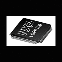
LPC2367FBD100 NXP Semiconductors, LPC2367FBD100 Datasheet - Page 49

LPC2367FBD100
Manufacturer Part Number
LPC2367FBD100
Description
The LPC2367FBD100 is a ARM7 microcontroller for embedded applications featuring a high level of integration and low power consumption at frequencies of 72 MHz
Manufacturer
NXP Semiconductors
Datasheet
1.LPC2364FET100.pdf
(69 pages)
Available stocks
Company
Part Number
Manufacturer
Quantity
Price
Company:
Part Number:
LPC2367FBD100
Manufacturer:
TI
Quantity:
160
Part Number:
LPC2367FBD100
Manufacturer:
ST
Quantity:
20 000
Company:
Part Number:
LPC2367FBD100,551
Manufacturer:
NXP Semiconductors
Quantity:
10 000
NXP Semiconductors
Table 10.
T
[1]
[2]
Table 11.
T
[1]
Table 12.
C
[1]
LPC2364_65_66_67_68
Product data sheet
Symbol
f
f
Symbol
t
t
Symbol
t
t
t
V
t
t
t
t
t
t
osc(RC)
i(RTC)
r
f
r
f
FRFM
FEOPT
FDEOP
JR1
JR2
EOPR1
EOPR2
amb
amb
L
CRS
= 50 pF; R
Parameters are valid over operating temperature range unless otherwise specified.
Typical ratings are not guaranteed. The values listed are at room temperature (25 C), nominal supply voltages.
Applies to standard I/O pins and RESET pin.
Characterized but not implemented as production test. Guaranteed by design.
= 40 C to +85 C; 3.0 V V
= 40 C to +85 C; V
Dynamic characteristic: internal oscillators
Dynamic characteristic: I/O pins
Dynamic characteristics of USB pins (full-speed) (LPC2364/66/68 only)
pu
= 1.5 k
11.1 Internal oscillators
11.2 I/O pins
11.3 USB interface
Parameter
internal RC oscillator frequency
RTC input frequency
Parameter
rise time
fall time
differential rise and fall time
matching
output signal crossover voltage
source SE0 interval of EOP
source jitter for differential transition
to SE0 transition
receiver jitter to next transition
receiver jitter for paired transitions
EOP width at receiver
EOP width at receiver
Parameter
rise time
fall time
on D+ to V
DD(3V3)
over specified ranges.
DD(3V3)
DD(3V3)
Conditions
pin configured as output
pin configured as output
All information provided in this document is subject to legal disclaimers.
3.6 V.
, unless otherwise specified.
[1]
Rev. 7 — 20 October 2011
[1]
Conditions
-
-
Conditions
10 % to 90 %
10 % to 90 %
see
see
10 % to 90 %
must reject as
EOP; see
Figure 14
must accept as
EOP; see
Figure 14
t
r
/ t
f
Figure 14
Figure 14
Min
3.0
2.5
LPC2364/65/66/67/68
Single-chip 16-bit/32-bit microcontrollers
Min
3.96
-
[1]
[1]
Min
7.7
-
1.3
160
2
18.5
9
40
82
8.5
Typ
-
-
Typ
-
-
-
-
-
-
-
-
-
-
Typ
4.02
32.768
[2]
© NXP B.V. 2011. All rights reserved.
Max
5.0
5.0
Max
13.8
13.7
109
2.0
175
+5
+18.5
+9
-
-
Max
4.04
-
Unit
ns
ns
MHz
Unit
ns
ns
%
V
ns
ns
ns
ns
ns
ns
49 of 69
Unit
kHz


