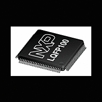
LPC2367FBD100 NXP Semiconductors, LPC2367FBD100 Datasheet - Page 32

LPC2367FBD100
Manufacturer Part Number
LPC2367FBD100
Description
The LPC2367FBD100 is a ARM7 microcontroller for embedded applications featuring a high level of integration and low power consumption at frequencies of 72 MHz
Manufacturer
NXP Semiconductors
Datasheet
1.LPC2364FET100.pdf
(69 pages)
Available stocks
Company
Part Number
Manufacturer
Quantity
Price
Company:
Part Number:
LPC2367FBD100
Manufacturer:
TI
Quantity:
160
Part Number:
LPC2367FBD100
Manufacturer:
ST
Quantity:
20 000
Company:
Part Number:
LPC2367FBD100,551
Manufacturer:
NXP Semiconductors
Quantity:
10 000
NXP Semiconductors
LPC2364_65_66_67_68
Product data sheet
7.24.1.1 Internal RC oscillator
7.24.1.2 Main oscillator
7.24.1.3 RTC oscillator
7.24.2 PLL
7.24.3 Wake-up timer
The IRC may be used as the clock source for the WDT, and/or as the clock that drives the
PLL and subsequently the CPU. The nominal IRC frequency is 4 MHz. The IRC is
trimmed to 1 % accuracy.
Upon power-up or any chip reset, the LPC2364/65/66/67/68 uses the IRC as the clock
source. Software may later switch to one of the other available clock sources.
The main oscillator can be used as the clock source for the CPU, with or without using the
PLL. The main oscillator operates at frequencies of 1 MHz to 25 MHz. This frequency can
be boosted to a higher frequency, up to the maximum CPU operating frequency, by the
PLL. The clock selected as the PLL input is PLLCLKIN. The ARM processor clock
frequency is referred to as CCLK elsewhere in this document. The frequencies of
PLLCLKIN and CCLK are the same value unless the PLL is active and connected. The
clock frequency for each peripheral can be selected individually and is referred to as
PCLK. Refer to
The RTC oscillator can be used as the clock source for the RTC and/or the WDT. Also, the
RTC oscillator can be used to drive the PLL and the CPU.
The PLL accepts an input clock frequency in the range of 32 kHz to 50 MHz. The input
frequency is multiplied up to a high frequency, then divided down to provide the actual
clock used by the CPU and the USB block. The USB block is available in LPC2364/66/68
only.
The PLL input, in the range of 32 kHz to 50 MHz, may initially be divided down by a value
‘N’, which may be in the range of 1 to 256. This input division provides a wide range of
output frequencies from the same input frequency.
Following the PLL input divider is the PLL multiplier. This can multiply the input divider
output through the use of a Current Controlled Oscillator (CCO) by a value ‘M’, in the
range of 1 through 32768. The resulting frequency must be in the range of 275 MHz to
550 MHz. The multiplier works by dividing the CCO output by the value of M, then using a
phase-frequency detector to compare the divided CCO output to the multiplier input. The
error value is used to adjust the CCO frequency.
The PLL is turned off and bypassed following a chip Reset and by entering Power-down
mode. PLL is enabled by software only. The program must configure and activate the PLL,
wait for the PLL to Lock, then connect to the PLL as a clock source.
The LPC2364/65/66/67/68 begins operation at power-up and when awakened from
Power-down and Deep power-down modes by using the 4 MHz IRC oscillator as the clock
source. This allows chip operation to resume quickly. If the main oscillator or the PLL is
needed by the application, software will need to enable these features and wait for them
to stabilize before they are used as a clock source.
All information provided in this document is subject to legal disclaimers.
Section 7.24.2
Rev. 7 — 20 October 2011
for additional information.
LPC2364/65/66/67/68
Single-chip 16-bit/32-bit microcontrollers
© NXP B.V. 2011. All rights reserved.
32 of 69


