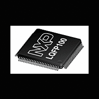
LPC2367FBD100 NXP Semiconductors, LPC2367FBD100 Datasheet - Page 36

LPC2367FBD100
Manufacturer Part Number
LPC2367FBD100
Description
The LPC2367FBD100 is a ARM7 microcontroller for embedded applications featuring a high level of integration and low power consumption at frequencies of 72 MHz
Manufacturer
NXP Semiconductors
Datasheet
1.LPC2364FET100.pdf
(69 pages)
Available stocks
Company
Part Number
Manufacturer
Quantity
Price
Company:
Part Number:
LPC2367FBD100
Manufacturer:
TI
Quantity:
160
Part Number:
LPC2367FBD100
Manufacturer:
ST
Quantity:
20 000
Company:
Part Number:
LPC2367FBD100,551
Manufacturer:
NXP Semiconductors
Quantity:
10 000
NXP Semiconductors
LPC2364_65_66_67_68
Product data sheet
CAUTION
7.25.3 Code security (Code Read Protection - CRP)
7.25.4 AHB
7.25.5 External interrupt inputs
This feature of the LPC2364/65/66/67/68 allows user to enable different levels of security
in the system so that access to the on-chip flash and use of the JTAG and ISP can be
restricted. When needed, CRP is invoked by programming a specific pattern into a
dedicated flash location. IAP commands are not affected by the CRP.
There are three levels of the Code Read Protection.
CRP1 disables access to chip via the JTAG and allows partial flash update (excluding
flash sector 0) using a limited set of the ISP commands. This mode is useful when CRP is
required and flash field updates are needed but all sectors can not be erased.
CRP2 disables access to chip via the JTAG and only allows full flash erase and update
using a reduced set of the ISP commands.
Running an application with level CRP3 selected fully disables any access to chip via the
JTAG pins and the ISP. This mode effectively disables ISP override using P2[10] pin, too.
It is up to the user’s application to provide (if needed) flash update mechanism using IAP
calls or call reinvoke ISP command to enable flash update via UART0.
The LPC2364/65/66/67/68 implement two AHBs in order to allow the Ethernet block to
operate without interference caused by other system activity. The primary AHB, referred
to as AHB1, includes the Vectored Interrupt Controller, GPDMA controller, USB interface,
and 8 kB SRAM primarily intended for use by the USB. The USB interface is available on
LPC2364/66/68 only.
The second AHB, referred to as AHB2, includes only the Ethernet block and an
associated 16 kB SRAM. In addition, a bus bridge is provided that allows the secondary
AHB to be a bus master on AHB1, allowing expansion of Ethernet buffer space into
unused space in memory residing on AHB1.
In summary, bus masters with access to AHB1 are the ARM7 itself, the USB block, the
GPDMA function, and the Ethernet block (via the bus bridge from AHB2). Bus masters
with access to AHB2 are the ARM7 and the Ethernet block.
The LPC2364/65/66/67/68 include up to 46 edge sensitive interrupt inputs combined with
up to four level sensitive external interrupt inputs as selectable pin functions. The external
interrupt inputs can optionally be used to wake up the processor from Power-down mode.
If level three Code Read Protection (CRP3) is selected, no future factory testing can be
performed on the device.
All information provided in this document is subject to legal disclaimers.
Rev. 7 — 20 October 2011
LPC2364/65/66/67/68
Single-chip 16-bit/32-bit microcontrollers
© NXP B.V. 2011. All rights reserved.
36 of 69


