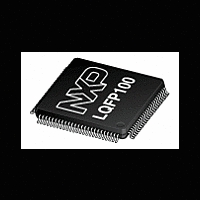
LPC2367FBD100 NXP Semiconductors, LPC2367FBD100 Datasheet - Page 35

LPC2367FBD100
Manufacturer Part Number
LPC2367FBD100
Description
The LPC2367FBD100 is a ARM7 microcontroller for embedded applications featuring a high level of integration and low power consumption at frequencies of 72 MHz
Manufacturer
NXP Semiconductors
Datasheet
1.LPC2364FET100.pdf
(69 pages)
Available stocks
Company
Part Number
Manufacturer
Quantity
Price
Company:
Part Number:
LPC2367FBD100
Manufacturer:
TI
Quantity:
160
Part Number:
LPC2367FBD100
Manufacturer:
ST
Quantity:
20 000
Company:
Part Number:
LPC2367FBD100,551
Manufacturer:
NXP Semiconductors
Quantity:
10 000
NXP Semiconductors
LPC2364_65_66_67_68
Product data sheet
7.25.1 Reset
7.25.2 Brownout detection
7.25 System control
The first option assumes that power consumption is not a concern and the design ties the
V
supply for both pads, the CPU, and peripherals. While this solution is simple, it does not
support powering down the I/O pad ring “on the fly” while keeping the CPU and
peripherals alive.
The second option uses two power supplies; a 3.3 V supply for the I/O pads (V
a dedicated 3.3 V supply for the CPU (V
converter powered independently from the I/O pad ring enables shutting down of the I/O
pad power supply “on the fly”, while the CPU and peripherals stay active.
The VBAT pin supplies power only to the RTC and the battery RAM. These two functions
require a minimum of power to operate, which can be supplied by an external battery.
When the CPU and the rest of chip functions are stopped and power removed, the RTC
can supply an alarm output that may be used by external hardware to restore chip power
and resume operation.
Reset has four sources on the LPC2364/65/66/67/68: the RESET pin, the Watchdog
reset, power-on reset, and the BrownOut Detection (BOD) circuit. The RESET pin is a
Schmitt trigger input pin. Assertion of chip Reset by any source, once the operating
voltage attains a usable level, starts the Wake-up timer (see description in
“Wake-up
de-asserted, the oscillator is running, a fixed number of clocks have passed, and the flash
controller has completed its initialization.
When the internal Reset is removed, the processor begins executing at address 0, which
is initially the Reset vector mapped from the Boot Block. At that point, all of the processor
and peripheral registers have been initialized to predetermined values.
The LPC2364/65/66/67/68 includes 2-stage monitoring of the voltage on the
V
to the Vectored Interrupt Controller. This signal can be enabled for interrupt in the Interrupt
Enable Register in the VIC in order to cause a CPU interrupt; if not, software can monitor
the signal by reading a dedicated status register.
The second stage of low-voltage detection asserts Reset to inactivate the
LPC2364/65/66/67/68 when the voltage on the V
Reset prevents alteration of the flash as operation of the various elements of the chip
would otherwise become unreliable due to low voltage. The BOD circuit maintains this
reset down below 1 V, at which point the power-on reset circuitry maintains the overall
Reset.
Both the 2.95 V and 2.65 V thresholds include some hysteresis. In normal operation, this
hysteresis allows the 2.95 V detection to reliably interrupt, or a regularly executed event
loop to sense the condition.
DD(3V3)
DD(DCDC)(3V3)
and V
timer”), causing reset to remain asserted until the external Reset is
DD(DCDC)(3V3)
pins. If this voltage falls below 2.95 V, the BOD asserts an interrupt signal
All information provided in this document is subject to legal disclaimers.
Rev. 7 — 20 October 2011
pins together. This approach requires only one 3.3 V power
DD(DCDC)(3V3)
LPC2364/65/66/67/68
Single-chip 16-bit/32-bit microcontrollers
DD(DCDC)(3V3)
). Having the on-chip DC-to-DC
pins falls below 2.65 V. This
© NXP B.V. 2011. All rights reserved.
Section 7.24.3
DD(3V3)
35 of 69
) and


