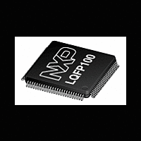
LPC2367FBD100 NXP Semiconductors, LPC2367FBD100 Datasheet - Page 28

LPC2367FBD100
Manufacturer Part Number
LPC2367FBD100
Description
The LPC2367FBD100 is a ARM7 microcontroller for embedded applications featuring a high level of integration and low power consumption at frequencies of 72 MHz
Manufacturer
NXP Semiconductors
Datasheet
1.LPC2364FET100.pdf
(69 pages)
Available stocks
Company
Part Number
Manufacturer
Quantity
Price
Company:
Part Number:
LPC2367FBD100
Manufacturer:
TI
Quantity:
160
Part Number:
LPC2367FBD100
Manufacturer:
ST
Quantity:
20 000
Company:
Part Number:
LPC2367FBD100,551
Manufacturer:
NXP Semiconductors
Quantity:
10 000
NXP Semiconductors
LPC2364_65_66_67_68
Product data sheet
7.18.1 Features
7.19.1 Features
7.19 I
The I
The I
and one word select signal. The basic I
master, and one slave. The I
separate transmit and receive channel, each of which can operate as either a master or a
slave.
2
•
•
•
•
•
•
•
•
•
•
•
•
•
•
•
•
•
•
•
S-bus serial I/O controllers
I
I
devices connected to the same bus lines.
Easy to configure as master, slave, or master/slave.
Programmable clocks allow versatile rate control.
Bidirectional data transfer between masters and slaves.
Multi-master bus (no central master).
Arbitration between simultaneously transmitting masters without corruption of serial
data on the bus.
Serial clock synchronization allows devices with different bit rates to communicate via
one serial bus.
Serial clock synchronization can be used as a handshake mechanism to suspend and
resume serial transfer.
The I
The interface has separate input/output channels each of which can operate in master
or slave mode.
Capable of handling 8-bit, 16-bit, and 32-bit word sizes.
Mono and stereo audio data supported.
The sampling frequency can range from 16 kHz to 48 kHz (16, 22.05, 32, 44.1,
48) kHz.
Configurable word select period in master mode (separately for I
Two 8-word FIFO data buffers are provided, one for transmit and one for receive.
Generates interrupt requests when buffer levels cross a programmable boundary.
Two DMA requests, controlled by programmable buffer levels. These are connected
to the GPDMA block.
Controls include reset, stop and mute options separately for I
2
2
2
2
C0 is a standard I
C1 and I
S-bus provides a standard communication interface for digital audio applications.
S-bus specification defines a 3-wire serial bus using one data line, one clock line,
2
C-bus can be used for test and diagnostic purposes.
2
C2 use standard I/O pins and do not support powering off of individual
All information provided in this document is subject to legal disclaimers.
Rev. 7 — 20 October 2011
2
C compliant bus interface with open-drain pins.
2
S interface on the LPC2364/65/66/67/68 provides a
2
S connection has one master, which is always the
LPC2364/65/66/67/68
Single-chip 16-bit/32-bit microcontrollers
2
S input and I
2
S input and output).
© NXP B.V. 2011. All rights reserved.
2
S output.
28 of 69


