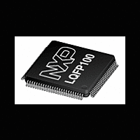
LPC2367FBD100 NXP Semiconductors, LPC2367FBD100 Datasheet - Page 19

LPC2367FBD100
Manufacturer Part Number
LPC2367FBD100
Description
The LPC2367FBD100 is a ARM7 microcontroller for embedded applications featuring a high level of integration and low power consumption at frequencies of 72 MHz
Manufacturer
NXP Semiconductors
Datasheet
1.LPC2364FET100.pdf
(69 pages)
Available stocks
Company
Part Number
Manufacturer
Quantity
Price
Company:
Part Number:
LPC2367FBD100
Manufacturer:
TI
Quantity:
160
Part Number:
LPC2367FBD100
Manufacturer:
ST
Quantity:
20 000
Company:
Part Number:
LPC2367FBD100,551
Manufacturer:
NXP Semiconductors
Quantity:
10 000
NXP Semiconductors
LPC2364_65_66_67_68
Product data sheet
7.2 On-chip flash programming memory
7.3 On-chip SRAM
7.4 Memory map
The key idea behind Thumb is that of a super-reduced instruction set. Essentially, the
ARM7TDMI-S processor has two instruction sets:
The Thumb set’s 16-bit instruction length allows it to approach twice the density of
standard ARM code while retaining most of the ARM’s performance advantage over a
traditional 16-bit processor using 16-bit registers. This is possible because Thumb code
operates on the same 32-bit register set as ARM code.
Thumb code is able to provide up to 65 % of the code size of ARM, and 160 % of the
performance of an equivalent ARM processor connected to a 16-bit memory system.
The LPC2364/65/66/67/68 incorporate a 128 kB, 256 kB, and 512 kB flash memory
system respectively. This memory may be used for both code and data storage.
Programming of the flash memory may be accomplished in several ways. It may be
programmed In System via the serial port (UART0). The application program may also
erase and/or program the flash while the application is running, allowing a great degree of
flexibility for data storage field and firmware upgrades.
The flash memory is 128 bits wide and includes pre-fetching and buffering techniques to
allow it to operate at SRAM speeds of 72 MHz. LPC2364HBD flash operates up to
72 MHz from 40 C to +85 C, up to 60 MHz from 85 C to 125 C.
The LPC2364/65/66/67/68 include SRAM memory of 8 kB or 32 kB, reserved for the ARM
processor exclusive use. This RAM may be used for code and/or data storage and may
be accessed as 8 bits, 16 bits, and 32 bits.
A 16 kB SRAM block serving as a buffer for the Ethernet controller and an 8 kB SRAM
used by the GPDMA controller or the USB device can be used both for data and code
storage. The 2 kB RTC SRAM can be used for data storage only. The RTC SRAM is
battery powered and retains the content in the absence of the main power supply.
The LPC2364/65/66/67/68 memory map incorporates several distinct regions as shown in
Figure
In addition, the CPU interrupt vectors may be remapped to allow them to reside in either
flash memory (default), boot ROM, or SRAM (see
•
•
The standard 32-bit ARM set
A 16-bit Thumb set
4.
All information provided in this document is subject to legal disclaimers.
Rev. 7 — 20 October 2011
LPC2364/65/66/67/68
Single-chip 16-bit/32-bit microcontrollers
Section
7.25.6).
© NXP B.V. 2011. All rights reserved.
19 of 69


