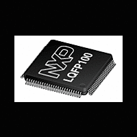
LPC2367FBD100 NXP Semiconductors, LPC2367FBD100 Datasheet - Page 17

LPC2367FBD100
Manufacturer Part Number
LPC2367FBD100
Description
The LPC2367FBD100 is a ARM7 microcontroller for embedded applications featuring a high level of integration and low power consumption at frequencies of 72 MHz
Manufacturer
NXP Semiconductors
Datasheet
1.LPC2364FET100.pdf
(69 pages)
Available stocks
Company
Part Number
Manufacturer
Quantity
Price
Company:
Part Number:
LPC2367FBD100
Manufacturer:
TI
Quantity:
160
Part Number:
LPC2367FBD100
Manufacturer:
ST
Quantity:
20 000
Company:
Part Number:
LPC2367FBD100,551
Manufacturer:
NXP Semiconductors
Quantity:
10 000
NXP Semiconductors
Table 4.
[1]
[2]
[3]
[4]
[5]
[6]
[7]
[8]
[9]
[10] Pad provides special analog functionality.
[11] When the main oscillator is not used, connect XTAL1 and XTAL2 as follows: XTAL1 can be left floating or can be grounded (grounding
LPC2364_65_66_67_68
Product data sheet
Symbol
RSTOUT
RESET
XTAL1
XTAL2
RTCX1
RTCX2
V
V
V
V
V
VREF
VBAT
SS
SSA
DD(3V3)
DD(DCDC)(3V3)
DDA
5 V tolerant pad providing digital I/O functions with TTL levels and hysteresis.
5 V tolerant pad providing digital I/O functions (with TTL levels and hysteresis) and analog input. When configured as a DAC input,
digital section of the pad is disabled.
5 V tolerant pad providing digital I/O with TTL levels and hysteresis and analog output function. When configured as the DAC output,
digital section of the pad is disabled.
Open-drain 5 V tolerant digital I/O pad, compatible with I
output functionality. When power is switched off, this pin connected to the I
Open-drain configuration applies to all functions on this pin.
Pad provides digital I/O and USB functions (LPC2364/66/68 only). It is designed in accordance with the USB specification, revision 2.0
(Full-speed and Low-speed mode only).
5 V tolerant pad with 5 ns glitch filter providing digital I/O functions with TTL levels and hysteresis.
This pin has no built-in pull-up and no built-in pull-down resistor.
This pin has a built-in pull-up resistor.
5 V tolerant pad with 20 ns glitch filter providing digital I/O function with TTL levels and hysteresis.
is preferred to reduce susceptibility to noise). XTAL2 should be left floating.
Pin description
Pin
14
17
22
23
16
18
15, 31,
41, 55,
72, 97,
83
11
28, 54,
71,
96
13, 42,
84
10
12
19
[14]
[9]
[10][11]
[10][11]
[10][12]
[10]
[13]
[15]
[16]
[17]
[17]
[17]
…continued
Ball
-
F3
H2
G3
F2
G1
B3, B7,
C9, F1,
G7, J6,
K3
E1
A3, C10,
H9,
K2
A7, E4,
H6
E2
E3
G2
[9]
[10][12]
[14]
[15]
[17]
[17]
[10][11]
[16]
[10][11]
[10]
[17]
[13]
Type
O
I
I
O
I
O
I
I
I
I
I
I
I
All information provided in this document is subject to legal disclaimers.
Description
RSTOUT — This is a 3.3 V pin. LOW on this pin indicates
LPC2364/65/66/67/68 being in Reset state.
Note: This pin is available in LPC2364FBD100, LPC2365FBD100,
LPC2366FBD100, LPC2367FBD100, and LPC2368FBD100 devices only
(LQFP100 package).
External reset input: A LOW on this pin resets the device, causing I/O
ports and peripherals to take on their default states, and processor
execution to begin at address 0. TTL with hysteresis, 5 V tolerant.
Input to the oscillator circuit and internal clock generator circuits.
Output from the oscillator amplifier.
Input to the RTC oscillator circuit.
Output from the RTC oscillator circuit.
ground: 0 V reference.
analog ground: 0 V reference. This should nominally be the same voltage
as V
3.3 V supply voltage: This is the power supply voltage for the I/O ports.
3.3 V DC-to-DC converter supply voltage: This is the supply voltage for
the on-chip DC-to-DC converter only.
analog 3.3 V pad supply voltage: This should be nominally the same
voltage as V
voltage is used to power the ADC and DAC.
ADC reference: This should be nominally the same voltage as V
should be isolated to minimize noise and error. Level on this pin is used as
a reference for ADC and DAC.
RTC pin power supply: 3.3 V on this pin supplies the power to the RTC
peripheral.
Rev. 7 — 20 October 2011
SS
2
C-bus 400 kHz specification. This pad requires an external pull-up to provide
, but should be isolated to minimize noise and error.
DD(3V3)
but should be isolated to minimize noise and error. This
2
C-bus is floating and does not disturb the I
LPC2364/65/66/67/68
Single-chip 16-bit/32-bit microcontrollers
© NXP B.V. 2011. All rights reserved.
2
C lines.
DD(3V3)
17 of 69
but


