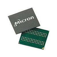
MT46H16M32LFCX-5:B Micron Technology Inc, MT46H16M32LFCX-5:B Datasheet - Page 26

MT46H16M32LFCX-5:B
Manufacturer Part Number
MT46H16M32LFCX-5:B
Description
IC DDR SDRAM 512MBIT 90VFBGA
Manufacturer
Micron Technology Inc
Type
DDR SDRAMr
Datasheet
1.MT46H16M32LFCX-5B.pdf
(98 pages)
Specifications of MT46H16M32LFCX-5:B
Format - Memory
RAM
Memory Type
Mobile DDR SDRAM
Memory Size
512M (16M x 32)
Speed
200MHz
Interface
Parallel
Voltage - Supply
1.7 V ~ 1.95 V
Operating Temperature
0°C ~ 70°C
Package / Case
90-VFBGA
Organization
16Mx32
Density
512Mb
Address Bus
15b
Access Time (max)
6.5/5ns
Maximum Clock Rate
200MHz
Operating Supply Voltage (typ)
1.8V
Package Type
VFBGA
Operating Temp Range
0C to 70C
Operating Supply Voltage (max)
1.95V
Operating Supply Voltage (min)
1.7V
Supply Current
125mA
Pin Count
90
Mounting
Surface Mount
Operating Temperature Classification
Commercial
Lead Free Status / RoHS Status
Lead free / RoHS Compliant
Available stocks
Company
Part Number
Manufacturer
Quantity
Price
Company:
Part Number:
MT46H16M32LFCX-5:B
Manufacturer:
Micron Technology Inc
Quantity:
10 000
Part Number:
MT46H16M32LFCX-5:B
Manufacturer:
MICRON
Quantity:
20 000
Company:
Part Number:
MT46H16M32LFCX-5:B TR
Manufacturer:
Micron Technology Inc
Quantity:
10 000
Electrical Specifications – AC Operating Conditions
Table 11: Electrical Characteristics and Recommended AC Operating Conditions
Notes 1–9 apply to all parameters in this table; V
PDF: 09005aef82d5d305
512mb_ddr_mobile_sdram_t47m.pdf – Rev. I 12/09 EN
Parameter
Access window
of DQ from
CK/CK#
Clock cycle time
CK high-level width
CK low-level width
CKE minimum pulse width
(high and low)
Auto precharge write recovery
+ precharge time
DQ and DM in-
put hold time
relative to DQS
DQ and DM in-
put hold time
relative to DQS
DQ and DM in-
put setup time
relative to DQ
DQ and DM in-
put setup time
relative to DQS
DQ and DM input pulse width
(for each input)
Access window
of DQS from
CK/CK#
DQS input high pulse width
DQS input low pulse width
DQS–DQ skew, DQS to last DQ
valid, per group, per access
WRITE command to first DQS
latching transition
DQS falling edge from CK
rising – hold time
DQS falling edge to CK rising –
setup time
Data valid output window
slow slew rate
slow slew rate
fast slew rate
fast slew rate
CL = 3
CL = 2
CL = 3
CL = 2
CL = 3
CL = 2
Symbol
t
DQSCK
t
t
t
t
t
DQSQ
DQSH
DVW
t
DIPW
t
t
DQSL
DQSS
t
t
t
t
t
t
t
DAL
DSH
t
CKE
t
DH
DH
DSS
DS
DS
AC
CK
CH
CL
f
s
f
s
Min
0.45
0.45
0.48
0.58
0.48
0.58
0.75
t
2.0
2.0
1.4
2.0
2.0
0.4
0.4
0.2
0.2
QH -
12
5
1
–
–
Electrical Specifications – AC Operating Conditions
DD
/V
-5
t
DQSQ
DDQ
Max
0.55
0.55
1.25
5.0
6.5
5.0
6.5
0.6
0.6
0.4
–
–
–
–
–
–
–
–
–
–
–
= 1.70–1.95V
26
Min
0.45
0.45
0.54
0.64
0.54
0.64
0.75
t
2.0
2.0
5.4
1.4
2.0
2.0
0.4
0.4
0.2
0.2
QH -
12
1
–
–
512Mb: x16, x32 Mobile LPDDR SDRAM
-54
t
DQSQ
Max
0.55
0.55
0.45
1.25
5.0
6.5
5.0
6.5
0.6
0.6
Micron Technology, Inc. reserves the right to change products or specifications without notice.
–
–
–
–
–
–
–
–
–
–
–
Min
0.45
0.45
0.75
t
2.0
2.0
0.6
0.7
0.6
0.7
1.4
2.0
2.0
0.4
0.4
0.2
0.2
QH -
12
6
1
–
–
-6
t
DQSQ
Max
0.55
0.55
1.25
5.0
6.5
5.0
6.5
0.6
0.6
0.5
–
–
–
–
–
–
–
–
–
–
–
Min
0.45
0.45
0.75
t
2.0
2.0
7.5
0.8
0.9
0.8
0.9
1.4
2.0
2.0
0.4
0.4
0.2
0.2
QH -
12
© 2004 Micron Technology, Inc. All rights reserved.
1
–
–
-75
t
DQSQ
Max
0.55
0.55
1.25
6.0
6.5
6.0
6.5
0.6
0.6
0.6
–
–
–
–
–
–
–
–
–
–
–
Unit Notes
t
t
t
t
t
t
t
t
ns
ns
CK
CK
CK
ns
ns
ns
ns
CK
CK
ns
CK
CK
CK
ns
13, 14,
13, 14,
13, 17
10
11
12
15
15
16
17


