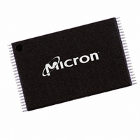
MT29F8G08FACWP:C TR Micron Technology Inc, MT29F8G08FACWP:C TR Datasheet - Page 17

MT29F8G08FACWP:C TR
Manufacturer Part Number
MT29F8G08FACWP:C TR
Description
IC FLASH 8GBIT 48TSOP
Manufacturer
Micron Technology Inc
Datasheet
1.MT29F2G08AACWPC_TR.pdf
(58 pages)
Specifications of MT29F8G08FACWP:C TR
Format - Memory
FLASH
Memory Type
FLASH - Nand
Memory Size
8G (1G x 8)
Interface
Parallel
Voltage - Supply
2.7 V ~ 3.6 V
Operating Temperature
0°C ~ 70°C
Package / Case
48-TSOP
Lead Free Status / RoHS Status
Lead free / RoHS Compliant
Speed
-
Data Input
READs
Ready/Busy#
PDF: 09005aef814b01a2 / Source: 09005aef814b01c7
2_4_8gb_nand_m49a__2.fm - Rev. D 12/06 EN
Where ΣI
Data is written to the data register on the rising edge of WE# when:
• CE#, CLE, and ALE are LOW, and
• the device is not busy.
Data is input on I/O[7:0] for x8 devices, and on I/O[15:0] for x16 devices. See Figure 36
on page 45 for additional data input details.
After a READ command is issued, data is transferred from the memory array to the data
register on the rising edge of WE#. R/B# goes LOW for
transfer is complete. When R/B# goes HIGH, data is available in the data register; it is
clocked out of the part by toggling RE#. See Figure 39 on page 46 for detailed timing
information.
The READ STATUS (70h) command or the R/B# signal can be used to determine when
the device is ready. See the READ STATUS command section on page 26 for details.
The R/B# output provides a hardware method of indicating the completion of PRO-
GRAM, ERASE, and READ operations. The signal requires a pull-up resistor for proper
operation. The signal is typically HIGH, and transitions to LOW after the appropriate
command is written to the device. The signal pin’s open-drain driver enables multiple
R/B# outputs to be OR-tied. The READ STATUS command can be used in place of R/B#.
Typically, R/B# is connected to an interrupt pin on the system controller (see Figure 11
on page 18).
On the 8Gb MT29F8G08FAC, R/B# provides a status indication for the 4Gb section
enabled by CE#, and R/B2# does the same for the 4Gb section enabled by CE2#. R/B#
and R/B2# can be tied together, or they can be used separately to provide independent
indications for each 4Gb section.
The combination of Rp and capacitive loading of the R/B# circuit determines the rise
time of the R/B# pin. The actual value used for Rp depends on the system timing
requirements. Large values of Rp cause R/B# to be delayed significantly. At the 10 per-
cent to 90 percent points on the R/B# waveform, rise time is approximately two time
constants (TC).
The fall time of the R/B# signal is determined mainly by the output impedance of the
R/B# pin and the total load capacitance.
Figure 12 on page 18 and Figure 13 on page 19 depict approximate Rp values using a cir-
cuit load of 100pF.
The minimum value for Rp is determined by the output drive capability of the R/B# sig-
nal, the output voltage swing, and V
Where R = Rp (resistance of pull-up resistor), and C = total capacitive load.
L
Rp MIN
is the sum of the input currents of all devices tied to the R/B# pin.
(
)
=
V
---------------------------------------------------------------
CC
(
MAX
TC
I
OL
) V
=
17
–
+
2Gb, 4Gb, 8Gb: x8, x16 NAND Flash Memory
R C
Σ
OL
IL
×
(
MAX
CC
.
Micron Technology, Inc., reserves the right to change products or specifications without notice.
)
=
------------------------- -
3mA
1.85V
+
Σ
IL
t
R and transitions HIGH after the
©2005 Micron Technology, Inc. All rights reserved.
Bus Operation


