OM11043 NXP Semiconductors, OM11043 Datasheet - Page 10
OM11043
Manufacturer Part Number
OM11043
Description
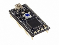
DEVELOPMENT BOARD LPC1768 MBED
Manufacturer
NXP Semiconductors
Series
mbedr
Type
MCUr
Specifications of OM11043
Contents
Board and software
Development Tool Type
Hardware / Software - Eval/Demo Board
Kit Contents
Board Cable Docs
Mcu Supported Families
LPC1000
Tool / Board Applications
General Purpose MCU, MPU, DSP, DSC
Silicon Manufacturer
NXP
Core Architecture
ARM
Core Sub-architecture
Cortex - M3
Silicon Core Number
LPC17xx
Silicon Family Name
LPC17xx
Lead Free Status / RoHS Status
Lead free / RoHS Compliant
For Use With/related Products
LPC1768
Lead Free Status / RoHS Status
Lead free / RoHS Compliant
Other names
568-4916
Available stocks
Company
Part Number
Manufacturer
Quantity
Price


NXP Semiconductors
Table 4.
LPC1769_68_67_66_65_64_63
Product data sheet
Symbol
P0[15]/TXD1/
SCK0/SCK
P0[16]/RXD1/
SSEL0/SSEL
P0[17]/CTS1/
MISO0/MISO
P0[18]/DCD1/
MOSI0/MOSI
P0[19]/DSR1/
SDA1
P0[20]/DTR1/SCL1 58
P0[21]/RI1/RD1
P0[22]/RTS1/TD1
P0[23]/AD0[0]/
I2SRX_CLK/
CAP3[0]
Pin description
Pin
62
63
61
60
59
57
56
9
[2]
[1]
[1]
[1]
[1]
[1]
[1]
[1]
[1]
…continued
Ball
F10
F8
F9
F6
G10
G9
G8
H10
E5
[1]
[1]
[1]
[2]
[1]
[1]
[1]
[1]
[1]
All information provided in this document is subject to legal disclaimers.
Type
I/O
O
I/O
I/O
I/O
I
I/O
I/O
I/O
I
I/O
I/O
I/O
I
I/O
I/O
I/O
I
I/O
I/O
O
I/O
I/O
I
I
I/O
O
O
I/O
I
I/O
I
Rev. 6.01 — 11 March 2011
Description
P0[15] — General purpose digital input/output pin.
TXD1 — Transmitter output for UART1.
SCK0 — Serial clock for SSP0.
SCK — Serial clock for SPI.
P0[16] — General purpose digital input/output pin.
RXD1 — Receiver input for UART1.
SSEL0 — Slave Select for SSP0.
SSEL — Slave Select for SPI.
P0[17] — General purpose digital input/output pin.
CTS1 — Clear to Send input for UART1.
MISO0 — Master In Slave Out for SSP0.
MISO — Master In Slave Out for SPI.
P0[18] — General purpose digital input/output pin.
DCD1 — Data Carrier Detect input for UART1.
MOSI0 — Master Out Slave In for SSP0.
MOSI — Master Out Slave In for SPI.
P0[19] — General purpose digital input/output pin.
DSR1 — Data Set Ready input for UART1.
SDA1 — I
open-drain pin).
P0[20] — General purpose digital input/output pin.
DTR1 — Data Terminal Ready output for UART1. Can also be
configured to be an RS-485/EIA-485 output enable signal.
SCL1 — I
open-drain pin).
P0[21] — General purpose digital input/output pin.
RI1 — Ring Indicator input for UART1.
RD1 — CAN1 receiver input. (LPC1769/68/66/65/64 only).
P0[22] — General purpose digital input/output pin.
RTS1 — Request to Send output for UART1. Can also be configured
to be an RS-485/EIA-485 output enable signal.
TD1 — CAN1 transmitter output. (LPC1769/68/66/65/64 only).
P0[23] — General purpose digital input/output pin.
AD0[0] — A/D converter 0, input 0.
I2SRX_CLK — Receive Clock. It is driven by the master and received
by the slave. Corresponds to the signal SCK in the I
specification. (LPC1769/68/67/66/65/63 only).
CAP3[0] — Capture input for Timer 3, channel 0.
LPC1769/68/67/66/65/64/63
2
2
C1 clock input/output (this is not an I
C1 data input/output (this is not an I
32-bit ARM Cortex-M3 microcontroller
2
2
C-bus compliant
C-bus compliant
© NXP B.V. 2011. All rights reserved.
2
S-bus
10 of 79
Related parts for OM11043
Image
Part Number
Description
Manufacturer
Datasheet
Request
R

Part Number:
Description:
NXP Semiconductors designed the LPC2420/2460 microcontroller around a 16-bit/32-bitARM7TDMI-S CPU core with real-time debug interfaces that include both JTAG andembedded trace
Manufacturer:
NXP Semiconductors
Datasheet:

Part Number:
Description:
NXP Semiconductors designed the LPC2458 microcontroller around a 16-bit/32-bitARM7TDMI-S CPU core with real-time debug interfaces that include both JTAG andembedded trace
Manufacturer:
NXP Semiconductors
Datasheet:
Part Number:
Description:
NXP Semiconductors designed the LPC2468 microcontroller around a 16-bit/32-bitARM7TDMI-S CPU core with real-time debug interfaces that include both JTAG andembedded trace
Manufacturer:
NXP Semiconductors
Datasheet:
Part Number:
Description:
NXP Semiconductors designed the LPC2470 microcontroller, powered by theARM7TDMI-S core, to be a highly integrated microcontroller for a wide range ofapplications that require advanced communications and high quality graphic displays
Manufacturer:
NXP Semiconductors
Datasheet:
Part Number:
Description:
NXP Semiconductors designed the LPC2478 microcontroller, powered by theARM7TDMI-S core, to be a highly integrated microcontroller for a wide range ofapplications that require advanced communications and high quality graphic displays
Manufacturer:
NXP Semiconductors
Datasheet:
Part Number:
Description:
The Philips Semiconductors XA (eXtended Architecture) family of 16-bit single-chip microcontrollers is powerful enough to easily handle the requirements of high performance embedded applications, yet inexpensive enough to compete in the market for hi
Manufacturer:
NXP Semiconductors
Datasheet:
Part Number:
Description:
The XA-S3 device is a member of Philips Semiconductors? XA(eXtended Architecture) family of high performance 16-bitsingle-chip microcontrollers
Manufacturer:
NXP Semiconductors
Datasheet:

Part Number:
Description:
The NXP BlueStreak LH75401/LH75411 family consists of two low-cost 16/32-bit System-on-Chip (SoC) devices
Manufacturer:
NXP Semiconductors
Datasheet:
Part Number:
Description:
The NXP LPC3130/3131 combine an 180 MHz ARM926EJ-S CPU core, high-speed USB2
Manufacturer:
NXP Semiconductors
Datasheet:
Part Number:
Description:
The NXP LPC3141 combine a 270 MHz ARM926EJ-S CPU core, High-speed USB 2
Manufacturer:
NXP Semiconductors
Part Number:
Description:
The NXP LPC3143 combine a 270 MHz ARM926EJ-S CPU core, High-speed USB 2
Manufacturer:
NXP Semiconductors

Part Number:
Description:
The NXP LPC3152 combines an 180 MHz ARM926EJ-S CPU core, High-speed USB 2
Manufacturer:
NXP Semiconductors
Part Number:
Description:
The NXP LPC3154 combines an 180 MHz ARM926EJ-S CPU core, High-speed USB 2
Manufacturer:
NXP Semiconductors

Part Number:
Description:
Standard level N-channel enhancement mode Field-Effect Transistor (FET) in a plastic package using NXP High-Performance Automotive (HPA) TrenchMOS technology
Manufacturer:
NXP Semiconductors
Datasheet: