OM11043 NXP Semiconductors, OM11043 Datasheet - Page 8
OM11043
Manufacturer Part Number
OM11043
Description
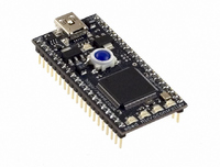
DEVELOPMENT BOARD LPC1768 MBED
Manufacturer
NXP Semiconductors
Series
mbedr
Type
MCUr
Specifications of OM11043
Contents
Board and software
Development Tool Type
Hardware / Software - Eval/Demo Board
Kit Contents
Board Cable Docs
Mcu Supported Families
LPC1000
Tool / Board Applications
General Purpose MCU, MPU, DSP, DSC
Silicon Manufacturer
NXP
Core Architecture
ARM
Core Sub-architecture
Cortex - M3
Silicon Core Number
LPC17xx
Silicon Family Name
LPC17xx
Lead Free Status / RoHS Status
Lead free / RoHS Compliant
For Use With/related Products
LPC1768
Lead Free Status / RoHS Status
Lead free / RoHS Compliant
Other names
568-4916
Available stocks
Company
Part Number
Manufacturer
Quantity
Price


NXP Semiconductors
Table 3.
Table 4.
LPC1769_68_67_66_65_64_63
Product data sheet
Pin Symbol
Row J
1
5
9
Row K
1
5
9
Symbol
P0[0] to P0[31]
P0[0]/RD1/TXD3/
SDA1
P0[1]/TD1/RXD3/
SCL1
P0[2]/TXD0/AD0[7] 98
P0[3]/RXD0/AD0[6] 99
P0[28]/SCL0/
USB_SCL
P1[22]/MCOB0/
USB_PWRD/
MAT1[0]
P2[13]/EINT3/
I2STX_SDA
P3[26]/STCLK/
MAT0[1]/PWM1[3]
P1[23]/MCI1/
PWM1[4]/MISO0
P0[11]/RXD2/
SCL2/MAT3[1]
Pin allocation table
Pin description
6.2 Pin description
Pin
46
47
[1]
[1]
[2]
[2]
Pin Symbol
2
6
10
2
6
10
Ball
K8
J8
C4
A2
…continued
[1]
[1]
[2]
[2]
P0[27]/SDA0/
USB_SDA
V
P2[10]/EINT0/NMI
V
P1[26]/MCOB1/
PWM1[6]/CAP0[0]
P2[12]/EINT2/
I2STX_WS
SS
DD(3V3)
All information provided in this document is subject to legal disclaimers.
Type
I/O
I/O
I
O
I/O
I/O
O
I
I/O
I/O
O
I
I/O
I
I
Rev. 6.01 — 11 March 2011
Description
Port 0: Port 0 is a 32-bit I/O port with individual direction controls for
each bit. The operation of port 0 pins depends upon the pin function
selected via the pin connect block. Pins 12, 13, 14, and 31 of this port
are not available.
P0[0] — General purpose digital input/output pin.
RD1 — CAN1 receiver input. (LPC1769/68/66/65/64 only).
TXD3 — Transmitter output for UART3.
SDA1 — I
open-drain pin).
P0[1] — General purpose digital input/output pin.
TD1 — CAN1 transmitter output. (LPC1769/68/66/65/64 only).
RXD3 — Receiver input for UART3.
SCL1 — I
open-drain pin).
P0[2] — General purpose digital input/output pin.
TXD0 — Transmitter output for UART0.
AD0[7] — A/D converter 0, input 7.
P0[3] — General purpose digital input/output pin.
RXD0 — Receiver input for UART0.
AD0[6] — A/D converter 0, input 6.
LPC1769/68/67/66/65/64/63
Pin Symbol
3
7
11
3
7
11
2
2
C1 clock input/output. (This is not an I
C1 data input/output. (This is not an I
P0[29]/USB_D+
P1[28]/MCOA2/
PCAP1[0]/
MAT0[0]
-
V
P1[27]/CLKOUT
/USB_OVRCR/
CAP0[1]
-
SS
32-bit ARM Cortex-M3 microcontroller
Pin Symbol
4
8
12
4
8
12
P1[19]/MCOA0/
USB_PPWR/
CAP1[1]
P0[1]/TD1/RXD3/SCL1
-
P1[20]/MCI0/
PWM1[2]/SCK0
P0[0]/RD1/TXD3/SDA1
-
2
2
C-bus compliant
C-bus compliant
© NXP B.V. 2011. All rights reserved.
8 of 79
Related parts for OM11043
Image
Part Number
Description
Manufacturer
Datasheet
Request
R

Part Number:
Description:
NXP Semiconductors designed the LPC2420/2460 microcontroller around a 16-bit/32-bitARM7TDMI-S CPU core with real-time debug interfaces that include both JTAG andembedded trace
Manufacturer:
NXP Semiconductors
Datasheet:

Part Number:
Description:
NXP Semiconductors designed the LPC2458 microcontroller around a 16-bit/32-bitARM7TDMI-S CPU core with real-time debug interfaces that include both JTAG andembedded trace
Manufacturer:
NXP Semiconductors
Datasheet:
Part Number:
Description:
NXP Semiconductors designed the LPC2468 microcontroller around a 16-bit/32-bitARM7TDMI-S CPU core with real-time debug interfaces that include both JTAG andembedded trace
Manufacturer:
NXP Semiconductors
Datasheet:
Part Number:
Description:
NXP Semiconductors designed the LPC2470 microcontroller, powered by theARM7TDMI-S core, to be a highly integrated microcontroller for a wide range ofapplications that require advanced communications and high quality graphic displays
Manufacturer:
NXP Semiconductors
Datasheet:
Part Number:
Description:
NXP Semiconductors designed the LPC2478 microcontroller, powered by theARM7TDMI-S core, to be a highly integrated microcontroller for a wide range ofapplications that require advanced communications and high quality graphic displays
Manufacturer:
NXP Semiconductors
Datasheet:
Part Number:
Description:
The Philips Semiconductors XA (eXtended Architecture) family of 16-bit single-chip microcontrollers is powerful enough to easily handle the requirements of high performance embedded applications, yet inexpensive enough to compete in the market for hi
Manufacturer:
NXP Semiconductors
Datasheet:
Part Number:
Description:
The XA-S3 device is a member of Philips Semiconductors? XA(eXtended Architecture) family of high performance 16-bitsingle-chip microcontrollers
Manufacturer:
NXP Semiconductors
Datasheet:

Part Number:
Description:
The NXP BlueStreak LH75401/LH75411 family consists of two low-cost 16/32-bit System-on-Chip (SoC) devices
Manufacturer:
NXP Semiconductors
Datasheet:
Part Number:
Description:
The NXP LPC3130/3131 combine an 180 MHz ARM926EJ-S CPU core, high-speed USB2
Manufacturer:
NXP Semiconductors
Datasheet:
Part Number:
Description:
The NXP LPC3141 combine a 270 MHz ARM926EJ-S CPU core, High-speed USB 2
Manufacturer:
NXP Semiconductors
Part Number:
Description:
The NXP LPC3143 combine a 270 MHz ARM926EJ-S CPU core, High-speed USB 2
Manufacturer:
NXP Semiconductors

Part Number:
Description:
The NXP LPC3152 combines an 180 MHz ARM926EJ-S CPU core, High-speed USB 2
Manufacturer:
NXP Semiconductors
Part Number:
Description:
The NXP LPC3154 combines an 180 MHz ARM926EJ-S CPU core, High-speed USB 2
Manufacturer:
NXP Semiconductors

Part Number:
Description:
Standard level N-channel enhancement mode Field-Effect Transistor (FET) in a plastic package using NXP High-Performance Automotive (HPA) TrenchMOS technology
Manufacturer:
NXP Semiconductors
Datasheet: