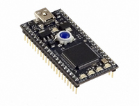
OM11043 NXP Semiconductors, OM11043 Datasheet - Page 40

OM11043
Manufacturer Part Number
OM11043
Description
DEVELOPMENT BOARD LPC1768 MBED
Manufacturer
NXP Semiconductors
Series
mbedr
Type
MCUr
Specifications of OM11043
Contents
Board and software
Development Tool Type
Hardware / Software - Eval/Demo Board
Kit Contents
Board Cable Docs
Mcu Supported Families
LPC1000
Tool / Board Applications
General Purpose MCU, MPU, DSP, DSC
Silicon Manufacturer
NXP
Core Architecture
ARM
Core Sub-architecture
Cortex - M3
Silicon Core Number
LPC17xx
Silicon Family Name
LPC17xx
Lead Free Status / RoHS Status
Lead free / RoHS Compliant
For Use With/related Products
LPC1768
Lead Free Status / RoHS Status
Lead free / RoHS Compliant
Other names
568-4916
Available stocks
Company
Part Number
Manufacturer
Quantity
Price
NXP Semiconductors
LPC1769_68_67_66_65_64_63
Product data sheet
CAUTION
7.30.2 Brownout detection
7.30.3 Code security (Code Read Protection - CRP)
7.30.4 APB interface
The LPC17xx include 2-stage monitoring of the voltage on the V
voltage falls below 2.2 V, the BOD asserts an interrupt signal to the Vectored Interrupt
Controller. This signal can be enabled for interrupt in the Interrupt Enable Register in the
NVIC in order to cause a CPU interrupt; if not, software can monitor the signal by reading
a dedicated status register.
The second stage of low-voltage detection asserts reset to inactivate the LPC17xx when
the voltage on the V
the flash as operation of the various elements of the chip would otherwise become
unreliable due to low voltage. The BOD circuit maintains this reset down below 1 V, at
which point the power-on reset circuitry maintains the overall reset.
Both the 2.2 V and 1.85 V thresholds include some hysteresis. In normal operation, this
hysteresis allows the 2.2 V detection to reliably interrupt, or a regularly executed event
loop to sense the condition.
This feature of the LPC17xx allows user to enable different levels of security in the system
so that access to the on-chip flash and use of the JTAG and ISP can be restricted. When
needed, CRP is invoked by programming a specific pattern into a dedicated flash location.
IAP commands are not affected by the CRP.
There are three levels of the Code Read Protection.
CRP1 disables access to chip via the JTAG and allows partial flash update (excluding
flash sector 0) using a limited set of the ISP commands. This mode is useful when CRP is
required and flash field updates are needed but all sectors can not be erased.
CRP2 disables access to chip via the JTAG and only allows full flash erase and update
using a reduced set of the ISP commands.
Running an application with level CRP3 selected fully disables any access to chip via the
JTAG pins and the ISP. This mode effectively disables ISP override using P2[10] pin, too.
It is up to the user’s application to provide (if needed) flash update mechanism using IAP
calls or call reinvoke ISP command to enable flash update via UART0.
The APB peripherals are split into two separate APB buses in order to distribute the bus
bandwidth and thereby reducing stalls caused by contention between the CPU and the
GPDMA controller.
If level three Code Read Protection (CRP3) is selected, no future factory testing can be
performed on the device.
All information provided in this document is subject to legal disclaimers.
DD(REG)(3V3)
Rev. 6.01 — 11 March 2011
pins falls below 1.85 V. This reset prevents alteration of
LPC1769/68/67/66/65/64/63
32-bit ARM Cortex-M3 microcontroller
DD(REG)(3V3)
© NXP B.V. 2011. All rights reserved.
pins. If this
40 of 79


