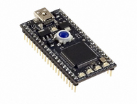
OM11043 NXP Semiconductors, OM11043 Datasheet - Page 30

OM11043
Manufacturer Part Number
OM11043
Description
DEVELOPMENT BOARD LPC1768 MBED
Manufacturer
NXP Semiconductors
Series
mbedr
Type
MCUr
Specifications of OM11043
Contents
Board and software
Development Tool Type
Hardware / Software - Eval/Demo Board
Kit Contents
Board Cable Docs
Mcu Supported Families
LPC1000
Tool / Board Applications
General Purpose MCU, MPU, DSP, DSC
Silicon Manufacturer
NXP
Core Architecture
ARM
Core Sub-architecture
Cortex - M3
Silicon Core Number
LPC17xx
Silicon Family Name
LPC17xx
Lead Free Status / RoHS Status
Lead free / RoHS Compliant
For Use With/related Products
LPC1768
Lead Free Status / RoHS Status
Lead free / RoHS Compliant
Other names
568-4916
Available stocks
Company
Part Number
Manufacturer
Quantity
Price
NXP Semiconductors
LPC1769_68_67_66_65_64_63
Product data sheet
7.22.1 Features
7.22 Pulse width modulator
The PWM is based on the standard Timer block and inherits all of its features, although
only the PWM function is pinned out on the LPC17xx. The Timer is designed to count
cycles of the system derived clock and optionally switch pins, generate interrupts or
perform other actions when specified timer values occur, based on seven match registers.
The PWM function is in addition to these features, and is based on match register events.
The ability to separately control rising and falling edge locations allows the PWM to be
used for more applications. For instance, multi-phase motor control typically requires
three non-overlapping PWM outputs with individual control of all three pulse widths and
positions.
Two match registers can be used to provide a single edge controlled PWM output. One
match register (PWMMR0) controls the PWM cycle rate, by resetting the count upon
match. The other match register controls the PWM edge position. Additional single edge
controlled PWM outputs require only one match register each, since the repetition rate is
the same for all PWM outputs. Multiple single edge controlled PWM outputs will all have a
rising edge at the beginning of each PWM cycle, when an PWMMR0 match occurs.
Three match registers can be used to provide a PWM output with both edges controlled.
Again, the PWMMR0 match register controls the PWM cycle rate. The other match
registers control the two PWM edge positions. Additional double edge controlled PWM
outputs require only two match registers each, since the repetition rate is the same for all
PWM outputs.
With double edge controlled PWM outputs, specific match registers control the rising and
falling edge of the output. This allows both positive going PWM pulses (when the rising
edge occurs prior to the falling edge), and negative going PWM pulses (when the falling
edge occurs prior to the rising edge).
•
•
•
•
Up to four external outputs corresponding to match registers, with the following
capabilities:
– Set LOW on match.
– Set HIGH on match.
– Toggle on match.
– Do nothing on match.
Up to two match registers can be used to generate timed DMA requests.
One PWM block with Counter or Timer operation (may use the peripheral clock or one
of the capture inputs as the clock source).
Seven match registers allow up to 6 single edge controlled or 3 double edge
controlled PWM outputs, or a mix of both types. The match registers also allow:
– Continuous operation with optional interrupt generation on match.
– Stop timer on match with optional interrupt generation.
– Reset timer on match with optional interrupt generation.
All information provided in this document is subject to legal disclaimers.
Rev. 6.01 — 11 March 2011
LPC1769/68/67/66/65/64/63
32-bit ARM Cortex-M3 microcontroller
© NXP B.V. 2011. All rights reserved.
30 of 79


