AT32UC3A0128-ALUT Atmel, AT32UC3A0128-ALUT Datasheet - Page 745
AT32UC3A0128-ALUT
Manufacturer Part Number
AT32UC3A0128-ALUT
Description
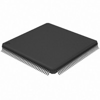
IC MCU AVR32 128KB FLASH 144LQFP
Manufacturer
Atmel
Series
AVR®32 UC3r
Specifications of AT32UC3A0128-ALUT
Core Processor
AVR
Core Size
32-Bit
Speed
66MHz
Connectivity
EBI/EMI, Ethernet, I²C, SPI, SSC, UART/USART, USB OTG
Peripherals
Brown-out Detect/Reset, POR, PWM, WDT
Number Of I /o
109
Program Memory Size
128KB (128K x 8)
Program Memory Type
FLASH
Ram Size
32K x 8
Voltage - Supply (vcc/vdd)
1.65 V ~ 1.95 V
Data Converters
A/D 8x10b
Oscillator Type
Internal
Operating Temperature
-40°C ~ 85°C
Package / Case
144-LQFP
Processor Series
AT32UC3x
Core
AVR32
Data Bus Width
32 bit
Data Ram Size
32 KB
Interface Type
2-Wire, RS-485, SPI, USART
Maximum Clock Frequency
66 MHz
Number Of Programmable I/os
69
Number Of Timers
3
Maximum Operating Temperature
+ 85 C
Mounting Style
SMD/SMT
3rd Party Development Tools
EWAVR32, EWAVR32-BL, KSK-EVK1100-PL
Development Tools By Supplier
ATAVRDRAGON, ATSTK500, ATSTK600, ATAVRISP2, ATAVRONEKIT, ATEXTWIFI, ATEVK1100, ATEVK1105
Minimum Operating Temperature
- 40 C
Controller Family/series
AT32UC3A
No. Of I/o's
109
Ram Memory Size
32KB
Cpu Speed
66MHz
No. Of Timers
1
Rohs Compliant
Yes
For Use With
ATEVK1105 - KIT EVAL FOR AT32UC3A0ATAVRONEKIT - KIT AVR/AVR32 DEBUGGER/PROGRMMR770-1008 - ISP 4PORT ATMEL AVR32 MCU SPIATEVK1100 - KIT DEV/EVAL FOR AVR32 AT32UC3A
Lead Free Status / RoHS Status
Lead free / RoHS Compliant
Eeprom Size
-
Lead Free Status / Rohs Status
Lead free / RoHS Compliant
Available stocks
Company
Part Number
Manufacturer
Quantity
Price
Company:

Part Number:
AT32UC3A0128-ALUT
Manufacturer:
Atmel
Quantity:
166


Figure 36-3. Scanning in JTAG instruction
36.6.2.2
36.6.3
32058J–AVR32–04/11
Boundary-Scan
Scanning in/out data
TCK
TAP State
TMS
TDI
TDO
TLR
At the TMS input, apply the sequence 1, 0, 0 at the rising edges of TCK to enter the Shift Data
Register - Shift-DR state. While in this state, upload the selected Data Register (selected by the
present JTAG instruction in the JTAG Instruction Register) from the TDI input at the rising edge
of TCK. In order to remain in the Shift-DR state, the TMS input must be held low. While the Data
Register is shifted in from the TDI pin, the parallel inputs to the Data Register captured in the
Capture-DR state is shifted out on the TDO pin.
Apply the TMS sequence 1, 1, 0 to re-enter the Run-Test/Idle state. If the selected Data Register
has a latched parallel-output, the latching takes place in the Update-DR state. The Exit-DR,
Pause-DR, and Exit2-DR states are only used for navigating the state machine.
As shown in the state diagram, the Run-Test/Idle state need not be entered between selecting
JTAG instruction and using Data Registers.
The Boundary-Scan chain has the capability of driving and observing the logic levels on the dig-
ital I/O pins, as well as the boundary between digital and analog logic for analog circuitry having
off-chip connections. At system level, all ICs having JTAG capabilities are connected serially by
the TDI/TDO signals to form a long shift register. An external controller sets up the devices to
drive values at their output pins, and observe the input values received from other devices. The
controller compares the received data with the expected result. In this way, Boundary-Scan pro-
vides a mechanism for testing interconnections and integrity of components on Printed Circuits
Boards by using the 4 TAP signals only.
The four IEEE 1149.1 defined mandatory JTAG instructions IDCODE, BYPASS, SAMPLE/PRE-
LOAD, and EXTEST can be used for testing the Printed Circuit Board. Initial scanning of the
data register path will show the ID-code of the device, since IDCODE is the default JTAG
instruction. It may be desirable to have the AVR32 device in reset during test mode. If not reset,
inputs to the device may be determined by the scan operations, and the internal software may
be in an undetermined state when exiting the test mode. Entering reset, the outputs of any Port
Pin will instantly enter the high impedance state, making the HIGHZ instruction redundant. If
needed, the BYPASS instruction can be issued to make the shortest possible scan chain
through the device. The device can be set in the reset state either by pulling the external
RESETn pin low, or issuing the AVR_RESET instruction with appropriate setting of the Reset
Data Register.
The EXTEST instruction is used for sampling external pins and loading output pins with data.
The data from the output latch will be driven out on the pins as soon as the EXTEST instruction
is loaded into the JTAG IR-register. Therefore, the SAMPLE/PRELOAD should also be used for
setting initial values to the scan ring, to avoid damaging the board when issuing the EXTEST
RTI
SelDR SelIR CapIR ShIR
Instruction
ImplDefined
Ex1IR UpdIR RTI
AT32UC3A
745
Related parts for AT32UC3A0128-ALUT
Image
Part Number
Description
Manufacturer
Datasheet
Request
R

Part Number:
Description:
DEV KIT FOR AVR/AVR32
Manufacturer:
Atmel
Datasheet:

Part Number:
Description:
INTERVAL AND WIPE/WASH WIPER CONTROL IC WITH DELAY
Manufacturer:
ATMEL Corporation
Datasheet:
Part Number:
Description:
Low-Voltage Voice-Switched IC for Hands-Free Operation
Manufacturer:
ATMEL Corporation
Datasheet:
Part Number:
Description:
MONOLITHIC INTEGRATED FEATUREPHONE CIRCUIT
Manufacturer:
ATMEL Corporation
Datasheet:
Part Number:
Description:
AM-FM Receiver IC U4255BM-M
Manufacturer:
ATMEL Corporation
Datasheet:
Part Number:
Description:
Monolithic Integrated Feature Phone Circuit
Manufacturer:
ATMEL Corporation
Datasheet:
Part Number:
Description:
Multistandard Video-IF and Quasi Parallel Sound Processing
Manufacturer:
ATMEL Corporation
Datasheet:
Part Number:
Description:
High-performance EE PLD
Manufacturer:
ATMEL Corporation
Datasheet:
Part Number:
Description:
8-bit Flash Microcontroller
Manufacturer:
ATMEL Corporation
Datasheet:
Part Number:
Description:
2-Wire Serial EEPROM
Manufacturer:
ATMEL Corporation
Datasheet: