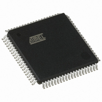
AT89C5132-ROTUL Atmel, AT89C5132-ROTUL Datasheet - Page 109

AT89C5132-ROTUL
Manufacturer Part Number
AT89C5132-ROTUL
Description
IC 8051 MCU FLASH 64K USB 80TQFP
Manufacturer
Atmel
Series
AT89C513xr
Specifications of AT89C5132-ROTUL
Core Processor
C52X2
Core Size
8-Bit
Speed
20MHz
Connectivity
IDE/ATAPI, I²C, MMC, PCM, SPI, UART/USART, USB
Peripherals
I²S, POR, WDT
Number Of I /o
44
Program Memory Size
64KB (64K x 8)
Program Memory Type
FLASH
Eeprom Size
4K x 8
Ram Size
2.25K x 8
Voltage - Supply (vcc/vdd)
2.7 V ~ 3.3 V
Data Converters
A/D 2x10b
Oscillator Type
Internal
Operating Temperature
-40°C ~ 85°C
Package / Case
80-TQFP, 80-VQFP
Cpu Family
89C
Device Core
8051
Device Core Size
8b
Frequency (max)
40MHz
Interface Type
IDE/SPI/UART/USB
Total Internal Ram Size
2.25KB
# I/os (max)
44
Number Of Timers - General Purpose
2
Operating Supply Voltage (typ)
3V
Operating Supply Voltage (max)
3.3V
Operating Supply Voltage (min)
2.7V
On-chip Adc
2-chx10-bit
Instruction Set Architecture
CISC
Operating Temp Range
-40C to 85C
Operating Temperature Classification
Industrial
Mounting
Surface Mount
Pin Count
80
Package Type
TQFP
Package
80TQFP
Family Name
89C
Maximum Speed
40 MHz
Operating Supply Voltage
3 V
Data Bus Width
8 Bit
Number Of Programmable I/os
44
Number Of Timers
2
Maximum Clock Frequency
20 MHz
Data Ram Size
2304 B
Mounting Style
SMD/SMT
A/d Bit Size
10 bit
A/d Channels Available
2
Height
1.45 mm
Length
14.1 mm
Maximum Operating Temperature
+ 85 C
Minimum Operating Temperature
- 40 C
Supply Voltage (max)
3.3 V
Supply Voltage (min)
2.7 V
Width
14.1 mm
For Use With
AT89OCD-01 - USB EMULATOR FOR AT8XC51 MCU
Lead Free Status / RoHS Status
Lead free / RoHS Compliant
Available stocks
Company
Part Number
Manufacturer
Quantity
Price
18.3.1
18.3.2
4173E–USB–09/07
Transmission
(Mode 0)
Reception
(Mode 0)
Figure 18-3. Serial I/O Port Block Diagram (Mode 0)
To start a transmission mode 0, write to SCON register clearing Bits SM0, SM1.
As shown in Figure 18-4, writing the byte to transmit to SBUF register starts the transmission.
Hardware shifts the LSB (D0) onto the RXD pin during the first clock cycle composed of a high
level then low level signal on TXD. During the eighth clock cycle the MSB (D7) is on the RXD
pin. Then, hardware drives the RXD pin high and asserts TI to indicate the end of the
transmission.
Figure 18-4. Transmission Waveforms (Mode 0)
To start a reception in mode 0, write to SCON register clearing SM0, SM1 and RI Bits and set-
ting the REN bit.
As shown in Figure 18-5, Clock is pulsed and the LSB (D0) is sampled on the RXD pin. The D0
bit is then shifted into the shift register. After eight sampling, the MSB (D7) is shifted into the shift
register, and hardware asserts RI bit to indicate a completed reception. Software can then read
the received byte from SBUF register.
Write to SBUF
SCON.6
SCON.1
M3 M2 M1 M0
SM1
Mode Decoder
TI
Controller
RXD
TXD
Mode
TI
SCON.7
SCON.0
SM0
RI
D0
D1
D2
D3
SBUF Rx SR
SBUF Tx SR
Baud Rate
Controller
D4
D5
D6
AT89C5132
D7
RXD
TXD
109


