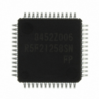
R5F21258SNFP#U0 Renesas Electronics America, R5F21258SNFP#U0 Datasheet - Page 107

R5F21258SNFP#U0
Manufacturer Part Number
R5F21258SNFP#U0
Description
IC R8C/25 MCU FLASH 52LQFP
Manufacturer
Renesas Electronics America
Series
R8C/2x/25r
Specifications of R5F21258SNFP#U0
Core Size
16/32-Bit
Program Memory Size
64KB (64K x 8)
Core Processor
R8C
Speed
20MHz
Connectivity
I²C, LIN, SIO, SSU, UART/USART
Peripherals
POR, Voltage Detect, WDT
Number Of I /o
41
Program Memory Type
FLASH
Ram Size
3K x 8
Voltage - Supply (vcc/vdd)
2.2 V ~ 5.5 V
Data Converters
A/D 12x10b
Oscillator Type
Internal
Operating Temperature
-20°C ~ 85°C
Package / Case
52-LQFP
No. Of I/o's
41
Ram Memory Size
3KB
Cpu Speed
20MHz
No. Of Timers
4
Digital Ic Case Style
LQFP
Supply Voltage Range
2.2V To 5.5V
Embedded Interface Type
I2C, UART
Rohs Compliant
Yes
Lead Free Status / RoHS Status
Lead free / RoHS Compliant
For Use With
YMCRPR8C25 - REF PLATFORM MOTOR CTRL R8C/25R0K521256S000BE - KIT EVAL STARTER FOR R8C/25
Eeprom Size
-
Lead Free Status / RoHS Status
Lead free / RoHS Compliant, Lead free / RoHS Compliant
Available stocks
Company
Part Number
Manufacturer
Quantity
Price
- Current page: 107 of 527
- Download datasheet (6Mb)
R8C/24 Group, R8C/25 Group
Rev.3.00
REJ09B0244-0300
10.5.1.1
10.5.1.2
10.5.1.3
10.5.1.4
The XIN clock divided by 1 (no division), 2, 4, 8, or 16 provides the CPU clock. Set the CM06 bit to 1 (divide-
by-8 mode) when transiting to high-speed on-chip oscillator mode, low-speed on-chip oscillator mode. If the
CM14 bit is set to 0 (low-speed on-chip oscillator on) or the FRA00 bit in the FRA0 register is set to 1 (high-
speed on-chip oscillator on), fOCO can be used as timer RA. When the FRA00 bit is set to 1, fOCO40M can be
used as timer RD. When the CM14 bit is set to 0 (low-speed on-chip oscillator on), fOCO-S can be used for the
watchdog timer and voltage detection circuit.
The XCIN clock divided by 1 (no division) provides the CPU clock.
In this mode, stopping the XIN clock and high-speed on-chip oscillator, and setting the FMR47 bit in the FMR4
register to 1 (flash memory low consumption current read mode enabled) enables low consumption operation.
When the FRA00 bit is set to 1, fOCO40M can be used as timer RD. When the CM14 bit is set to 0 (low-speed
on-chip oscillator on), fOCO-S can be used for the watchdog timer and voltage detection circuit.
To enter wait mode from low-speed clock mode, setting the VCA20 bit in the VCA2 register to 1 (internal
power low consumption enabled) enables lower consumption current in wait mode.
When enabling reduced internal power consumption using the VCA20 bit, follow Figure 10.13 Procedure for
Enabling Reduced Internal Power Consumption Using VCA20 bit.
The high-speed on-chip oscillator is used as the on-chip oscillator clock when the FRA00 bit in the FRA0
register is set to 1 (high-speed on-chip oscillator on) and the FRA01 bit in the FRA0 register is set to 1. The on-
chip oscillator divided by 1 (no division), 2, 4, 8, or 16 provides the CPU clock. Set the CM06 bit to 1 (divide-
by-8 mode) when transiting to high-speed clock mode. If the FRA00 bit is set to 1, fOCO40M can be used as
timer RD. When the CM14 bit is set to 0 (low-speed on-chip oscillator on), fOCO-S can be used for the
watchdog timer and voltage detection circuit.
If the CM14 bit in the CM1 register is set to 0 (low-speed on-chip oscillator on) or the FRA01bit in the FRA0
register is set to 0, the low-speed on-chip oscillator provides the on-chip oscillator clock.
The on-chip oscillator clock divided by 1 (no division), 2, 4, 8 or 16 provides the CPU clock. The on-chip
oscillator clock is also the clock source for the peripheral function clocks. Set the CM06 bit to 1 (divide-by-8
mode) when transiting to high-speed clock mode. When the FRA00 bit is set to 1, fOCO40M can be used as
timer RD. When the CM14 bit is set to 0 (low-speed on-chip oscillator on), fOCO-S can be used as the
watchdog timer and voltage detection circuit.
In this mode, stopping the XIN clock and high-speed on-chip oscillator, and setting the FMR47 bit in the FMR4
register to 1 (flash memory low consumption current read mode enabled) enables low consumption operation.
To enter wait mode from low-speed on-chip oscillator mode, setting the VCA20 bit in the VCA2 register to 1
(internal power low consumption enabled) enables lower consumption current in wait mode.
When enabling reduced internal power consumption using the VCA20 bit, follow Figure 10.13 Procedure for
Enabling Reduced Internal Power Consumption Using VCA20 bit.
Feb 29, 2008
High-Speed Clock Mode
Low-Speed Clock Mode
High-Speed On-Chip Oscillator Mode
Low-Speed On-Chip Oscillator Mode
Page 88 of 485
10. Clock Generation Circuit
Related parts for R5F21258SNFP#U0
Image
Part Number
Description
Manufacturer
Datasheet
Request
R

Part Number:
Description:
KIT STARTER FOR M16C/29
Manufacturer:
Renesas Electronics America
Datasheet:

Part Number:
Description:
KIT STARTER FOR R8C/2D
Manufacturer:
Renesas Electronics America
Datasheet:

Part Number:
Description:
R0K33062P STARTER KIT
Manufacturer:
Renesas Electronics America
Datasheet:

Part Number:
Description:
KIT STARTER FOR R8C/23 E8A
Manufacturer:
Renesas Electronics America
Datasheet:

Part Number:
Description:
KIT STARTER FOR R8C/25
Manufacturer:
Renesas Electronics America
Datasheet:

Part Number:
Description:
KIT STARTER H8S2456 SHARPE DSPLY
Manufacturer:
Renesas Electronics America
Datasheet:

Part Number:
Description:
KIT STARTER FOR R8C38C
Manufacturer:
Renesas Electronics America
Datasheet:

Part Number:
Description:
KIT STARTER FOR R8C35C
Manufacturer:
Renesas Electronics America
Datasheet:

Part Number:
Description:
KIT STARTER FOR R8CL3AC+LCD APPS
Manufacturer:
Renesas Electronics America
Datasheet:

Part Number:
Description:
KIT STARTER FOR RX610
Manufacturer:
Renesas Electronics America
Datasheet:

Part Number:
Description:
KIT STARTER FOR R32C/118
Manufacturer:
Renesas Electronics America
Datasheet:

Part Number:
Description:
KIT DEV RSK-R8C/26-29
Manufacturer:
Renesas Electronics America
Datasheet:

Part Number:
Description:
KIT STARTER FOR SH7124
Manufacturer:
Renesas Electronics America
Datasheet:

Part Number:
Description:
KIT STARTER FOR H8SX/1622
Manufacturer:
Renesas Electronics America
Datasheet:

Part Number:
Description:
KIT DEV FOR SH7203
Manufacturer:
Renesas Electronics America
Datasheet:


