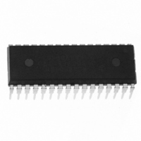
MC68HC908JL8CSPE Freescale Semiconductor, MC68HC908JL8CSPE Datasheet - Page 123

MC68HC908JL8CSPE
Manufacturer Part Number
MC68HC908JL8CSPE
Description
IC MCU 8K FLASH 8MHZ 32-DIP
Manufacturer
Freescale Semiconductor
Series
HC08r
Specifications of MC68HC908JL8CSPE
Core Processor
HC08
Core Size
8-Bit
Speed
8MHz
Connectivity
SCI
Peripherals
LED, LVD, POR, PWM
Number Of I /o
26
Program Memory Size
8KB (8K x 8)
Program Memory Type
FLASH
Ram Size
256 x 8
Voltage - Supply (vcc/vdd)
2.7 V ~ 5.5 V
Data Converters
A/D 13x8b
Oscillator Type
Internal
Operating Temperature
-40°C ~ 85°C
Package / Case
32-SDIP (0.400", 10.16mm)
Controller Family/series
HC08
No. Of I/o's
26
Ram Memory Size
256Byte
Cpu Speed
8MHz
No. Of Timers
2
Embedded Interface Type
I2C, SCI, SPI
Rohs Compliant
Yes
Processor Series
HC08JL
Core
HC08
Data Bus Width
8 bit
Data Ram Size
256 B
Interface Type
SCI
Maximum Clock Frequency
8 MHz
Number Of Programmable I/os
26
Number Of Timers
4
Operating Supply Voltage
0 V to 5 V
Maximum Operating Temperature
+ 125 C
Mounting Style
Through Hole
Development Tools By Supplier
FSICEBASE, DEMO908JL16E, M68CBL05CE
Minimum Operating Temperature
- 40 C
On-chip Adc
8 bit, 13 Channel
Lead Free Status / RoHS Status
Lead free / RoHS Compliant
Eeprom Size
-
Lead Free Status / Rohs Status
Details
Available stocks
Company
Part Number
Manufacturer
Quantity
Price
Company:
Part Number:
MC68HC908JL8CSPE
Manufacturer:
SINOPOWER
Quantity:
24 000
Company:
Part Number:
MC68HC908JL8CSPE
Manufacturer:
Freescale Semiconductor
Quantity:
135
Company:
Part Number:
MC68HC908JL8CSPE
Manufacturer:
FREESCALE
Quantity:
51
Part Number:
MC68HC908JL8CSPE
Manufacturer:
FREESCALE
Quantity:
20 000
9.4 Functional Description
Figure 9-1
communication among the MCU and remote devices, including other MCUs. The transmitter and receiver
of the SCI operate independently, although they use the same baud rate generator. During normal
operation, the CPU monitors the status of the SCI, writes the data to be transmitted, and processes
received data. The baud rate clock source for the SCI is the bus clock.
9.4.1 Data Format
The SCI uses the standard non-return-to-zero mark/space data format illustrated in
Freescale Semiconductor
$0014
$0015
$0016 SCI Status Register 1 (SCS1)
$0017 SCI Status Register 2 (SCS2)
$0018
$0019
Addr.
$0013
SCI Baud Rate Register
shows the structure of the SCI module. The SCI allows full-duplex, asynchronous, NRZ serial
Register Name
SCI Control Register 1
SCI Control Register 2
SCI Control Register 3
SCI Data Register
START
START
BIT
BIT
MC68HC908JL8/JK8 • MC68HC08JL8/JK8 • MC68HC908KL8 Data Sheet, Rev. 3.1
(SCDR)
(SCBR)
BIT 0
BIT 0
(SCC1)
(SCC2)
(SCC3)
BIT 1
BIT 1
Reset:
Reset:
Reset:
Reset:
Reset:
Reset:
Reset:
Read:
Read:
Read:
Read:
Read:
Read:
Read:
Write:
Write:
Write:
Write:
Write:
Write:
Write:
Figure 9-2. SCI I/O Register Summary
BIT 2
BIT 2
LOOPS
SCTIE
SCTE
Bit 7
R8
R7
T7
Figure 9-3. SCI Data Formats
U
0
0
1
0
0
0
BIT 3
BIT 3
BIT M IN SCC1 CLEAR
8-BIT DATA FORMAT
= Unimplemented
9-BIT DATA FORMAT
BIT M IN SCC1 SET
ENSCI
TCIE
TC
R6
T8
T6
BIT 4
BIT 4
U
6
0
0
1
0
0
0
BIT 5
BIT 5
DMARE
SCRIE
TXINV
SCRF
SCP1
R5
T5
5
0
0
0
0
0
0
BIT 6
BIT 6
R = Reserved
DMATE
Unaffected by reset
SCP0
IDLE
ILIE
PARITY
R4
T4
M
BIT 7
BIT 7
4
0
0
0
0
0
0
BIT
PARITY
STOP
BIT 8
BIT
BIT
WAKE
ORIE
OR
TE
R3
T3
R
3
0
0
0
0
0
0
START
STOP
NEXT
BIT
BIT
U = Unaffected
SCR2
NEIE
ILTY
RE
NF
R2
T2
START
2
0
0
0
0
0
0
NEXT
BIT
Functional Description
Figure
SCR1
RWU
FEIE
PEN
BKF
FE
R1
T1
1
0
0
0
0
0
0
9-3.
SCR0
PEIE
Bit 0
PTY
SBK
RPF
PE
R0
T0
0
0
0
0
0
0
123


