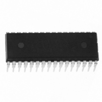
MC68HC908JL8CSPE Freescale Semiconductor, MC68HC908JL8CSPE Datasheet - Page 147

MC68HC908JL8CSPE
Manufacturer Part Number
MC68HC908JL8CSPE
Description
IC MCU 8K FLASH 8MHZ 32-DIP
Manufacturer
Freescale Semiconductor
Series
HC08r
Specifications of MC68HC908JL8CSPE
Core Processor
HC08
Core Size
8-Bit
Speed
8MHz
Connectivity
SCI
Peripherals
LED, LVD, POR, PWM
Number Of I /o
26
Program Memory Size
8KB (8K x 8)
Program Memory Type
FLASH
Ram Size
256 x 8
Voltage - Supply (vcc/vdd)
2.7 V ~ 5.5 V
Data Converters
A/D 13x8b
Oscillator Type
Internal
Operating Temperature
-40°C ~ 85°C
Package / Case
32-SDIP (0.400", 10.16mm)
Controller Family/series
HC08
No. Of I/o's
26
Ram Memory Size
256Byte
Cpu Speed
8MHz
No. Of Timers
2
Embedded Interface Type
I2C, SCI, SPI
Rohs Compliant
Yes
Processor Series
HC08JL
Core
HC08
Data Bus Width
8 bit
Data Ram Size
256 B
Interface Type
SCI
Maximum Clock Frequency
8 MHz
Number Of Programmable I/os
26
Number Of Timers
4
Operating Supply Voltage
0 V to 5 V
Maximum Operating Temperature
+ 125 C
Mounting Style
Through Hole
Development Tools By Supplier
FSICEBASE, DEMO908JL16E, M68CBL05CE
Minimum Operating Temperature
- 40 C
On-chip Adc
8 bit, 13 Channel
Lead Free Status / RoHS Status
Lead free / RoHS Compliant
Eeprom Size
-
Lead Free Status / Rohs Status
Details
Available stocks
Company
Part Number
Manufacturer
Quantity
Price
Company:
Part Number:
MC68HC908JL8CSPE
Manufacturer:
SINOPOWER
Quantity:
24 000
Company:
Part Number:
MC68HC908JL8CSPE
Manufacturer:
Freescale Semiconductor
Quantity:
135
Company:
Part Number:
MC68HC908JL8CSPE
Manufacturer:
FREESCALE
Quantity:
51
Part Number:
MC68HC908JL8CSPE
Manufacturer:
FREESCALE
Quantity:
20 000
Interrupts
10.3.2 Voltage Conversion
When the input voltage to the ADC equals V
, the ADC converts the signal to $FF (full scale). If the input
DD
voltage equals V
, the ADC converts it to $00. Input voltages between V
and V
are a straight-line
SS
DD
SS
linear conversion. All other input voltages will result in $FF if greater than V
and $00 if less than V
.
DD
SS
NOTE
Input voltage should not exceed the analog supply voltages.
10.3.3 Conversion Time
Fourteen ADC internal clocks are required to perform one conversion. The ADC starts a conversion on
the first rising edge of the ADC internal clock immediately following a write to the ADSCR. If the ADC
internal clock is selected to run at 1MHz, then one conversion will take 14µs to complete. With a 1MHz
ADC internal clock the maximum sample rate is 71.43kHz.
14 ADC Clock Cycles
Conversion Time =
ADC Clock Frequency
Number of Bus Cycles = Conversion Time × Bus Frequency
10.3.4 Continuous Conversion
In the continuous conversion mode, the ADC continuously converts the selected channel filling the ADC
data register with new data after each conversion. Data from the previous conversion will be overwritten
whether that data has been read or not. Conversions will continue until the ADCO bit is cleared. The
COCO bit (ADC status and control register, $003C) is set after each conversion and can be cleared by
writing the ADC status and control register or reading of the ADC data register.
10.3.5 Accuracy and Precision
The conversion process is monotonic and has no missing codes.
10.4 Interrupts
When the AIEN bit is set, the ADC module is capable of generating a CPU interrupt after each ADC
conversion. A CPU interrupt is generated if the COCO bit is at logic 0. The COCO bit is not used as a
conversion complete flag when interrupts are enabled.
10.5 Low-Power Modes
The following subsections describe the ADC in low-power modes.
10.5.1 Wait Mode
The ADC continues normal operation during wait mode. Any enabled CPU interrupt request from the ADC
can bring the MCU out of wait mode. If the ADC is not required to bring the MCU out of wait mode, power
down the ADC by setting the ADCH[4:0] bits in the ADC status and control register to logic 1’s before
executing the WAIT instruction.
MC68HC908JL8/JK8 • MC68HC08JL8/JK8 • MC68HC908KL8 Data Sheet, Rev. 3.1
Freescale Semiconductor
147


