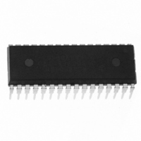
MC68HC908JL8CSPE Freescale Semiconductor, MC68HC908JL8CSPE Datasheet - Page 194

MC68HC908JL8CSPE
Manufacturer Part Number
MC68HC908JL8CSPE
Description
IC MCU 8K FLASH 8MHZ 32-DIP
Manufacturer
Freescale Semiconductor
Series
HC08r
Specifications of MC68HC908JL8CSPE
Core Processor
HC08
Core Size
8-Bit
Speed
8MHz
Connectivity
SCI
Peripherals
LED, LVD, POR, PWM
Number Of I /o
26
Program Memory Size
8KB (8K x 8)
Program Memory Type
FLASH
Ram Size
256 x 8
Voltage - Supply (vcc/vdd)
2.7 V ~ 5.5 V
Data Converters
A/D 13x8b
Oscillator Type
Internal
Operating Temperature
-40°C ~ 85°C
Package / Case
32-SDIP (0.400", 10.16mm)
Controller Family/series
HC08
No. Of I/o's
26
Ram Memory Size
256Byte
Cpu Speed
8MHz
No. Of Timers
2
Embedded Interface Type
I2C, SCI, SPI
Rohs Compliant
Yes
Processor Series
HC08JL
Core
HC08
Data Bus Width
8 bit
Data Ram Size
256 B
Interface Type
SCI
Maximum Clock Frequency
8 MHz
Number Of Programmable I/os
26
Number Of Timers
4
Operating Supply Voltage
0 V to 5 V
Maximum Operating Temperature
+ 125 C
Mounting Style
Through Hole
Development Tools By Supplier
FSICEBASE, DEMO908JL16E, M68CBL05CE
Minimum Operating Temperature
- 40 C
On-chip Adc
8 bit, 13 Channel
Lead Free Status / RoHS Status
Lead free / RoHS Compliant
Eeprom Size
-
Lead Free Status / Rohs Status
Details
Available stocks
Company
Part Number
Manufacturer
Quantity
Price
Company:
Part Number:
MC68HC908JL8CSPE
Manufacturer:
SINOPOWER
Quantity:
24 000
Company:
Part Number:
MC68HC908JL8CSPE
Manufacturer:
Freescale Semiconductor
Quantity:
135
Company:
Part Number:
MC68HC908JL8CSPE
Manufacturer:
FREESCALE
Quantity:
51
Part Number:
MC68HC908JL8CSPE
Manufacturer:
FREESCALE
Quantity:
20 000
Electrical Specifications
17.14 Memory Characteristics
194
RAM
FLASH program bus clock frequency
FLASH
FLASH
FLASH
FLASH PGM
FLASH
FLASH
FLASH
FLASH
FLASH
FLASH
FLASH
FLASH
FLASH
1. f
2. If the page erase time is longer than t
3. If the mass erase time is longer than t
4. t
5. t
6. The minimum row endurance value specifies each row of the FLASH memory is guaranteed to work for at least this many
7. The minimum row endurance value specifies each row of the FLASH memory is guaranteed to work for at least this many
8. The FLASH is guaranteed to retain data over the entire operating temperature range for at least the minimum time speci-
memory.
memory.
HVEN to logic 0.
t
erase / program cycles.
erase / program cycles.
fied.
rcv
read
HV
HV
data retention voltage
is defined as the time it needs before the FLASH can be read after turning off the high voltage charge pump, by clearing
is defined as the cumulative high voltage programming time to the same row before next erase.
must satisfy this condition: t
is defined as the frequency range for which the FLASH memory can be read.
read bus clock frequency
page erase time
mass erase time
high-voltage hold time
high-voltage hold time (mass erase)
program hold time
program time
return to read time
cumulative program hv period
row erase enduran
row program end
data retention t
/
ERASE
MC68HC908JL8/JK8 • MC68HC08JL8/JK8 • MC68HC908KL8 Data Sheet, Rev. 3.1
Characteristic
ime
to
urance
HVEN
ce
(8)
(6)
(7)
set up time
nvs
+ t
Table 17-12. Memory Characteristics
nvh
merase
erase
+ t
pgs
(Min), there is no erase-disturb, but it reduces the endurance of the FLASH
(Min), there is no erase-disturb, but it reduces the endurance of the FLASH
+ (t
prog
×
32) ≤ t
t
HV
Symbol
me
t
f
V
e
t
t
r
t
t
rcv
HV
rase
t
t
ead
t
prog
nvhl
RDR
—
nvh
pgs
—
—
—
rase
nvs
max.
(4)
(5)
(1)
(2)
(3)
32k
100
10k
10k
Min
1.3
10
30
10
—
1
4
4
5
5
1
Freescale Semiconductor
Max
8M
40
—
—
—
—
—
—
—
—
—
—
—
—
4
cycles
cycles
years
MHz
Unit
ms
ms
ms
Hz
µs
µs
µs
µs
µs
µs
V


