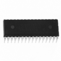
MC68HC908JL8CSPE Freescale Semiconductor, MC68HC908JL8CSPE Datasheet - Page 137

MC68HC908JL8CSPE
Manufacturer Part Number
MC68HC908JL8CSPE
Description
IC MCU 8K FLASH 8MHZ 32-DIP
Manufacturer
Freescale Semiconductor
Series
HC08r
Specifications of MC68HC908JL8CSPE
Core Processor
HC08
Core Size
8-Bit
Speed
8MHz
Connectivity
SCI
Peripherals
LED, LVD, POR, PWM
Number Of I /o
26
Program Memory Size
8KB (8K x 8)
Program Memory Type
FLASH
Ram Size
256 x 8
Voltage - Supply (vcc/vdd)
2.7 V ~ 5.5 V
Data Converters
A/D 13x8b
Oscillator Type
Internal
Operating Temperature
-40°C ~ 85°C
Package / Case
32-SDIP (0.400", 10.16mm)
Controller Family/series
HC08
No. Of I/o's
26
Ram Memory Size
256Byte
Cpu Speed
8MHz
No. Of Timers
2
Embedded Interface Type
I2C, SCI, SPI
Rohs Compliant
Yes
Processor Series
HC08JL
Core
HC08
Data Bus Width
8 bit
Data Ram Size
256 B
Interface Type
SCI
Maximum Clock Frequency
8 MHz
Number Of Programmable I/os
26
Number Of Timers
4
Operating Supply Voltage
0 V to 5 V
Maximum Operating Temperature
+ 125 C
Mounting Style
Through Hole
Development Tools By Supplier
FSICEBASE, DEMO908JL16E, M68CBL05CE
Minimum Operating Temperature
- 40 C
On-chip Adc
8 bit, 13 Channel
Lead Free Status / RoHS Status
Lead free / RoHS Compliant
Eeprom Size
-
Lead Free Status / Rohs Status
Details
Available stocks
Company
Part Number
Manufacturer
Quantity
Price
Company:
Part Number:
MC68HC908JL8CSPE
Manufacturer:
SINOPOWER
Quantity:
24 000
Company:
Part Number:
MC68HC908JL8CSPE
Manufacturer:
Freescale Semiconductor
Quantity:
135
Company:
Part Number:
MC68HC908JL8CSPE
Manufacturer:
FREESCALE
Quantity:
51
Part Number:
MC68HC908JL8CSPE
Manufacturer:
FREESCALE
Quantity:
20 000
TE — Transmitter Enable Bit
RE — Receiver Enable Bit
RWU — Receiver Wakeup Bit
SBK — Send Break Bit
Freescale Semiconductor
Setting this read/write bit begins the transmission by sending a preamble of 10 or 11 logic 1s from the
transmit shift register to the TxD pin. If software clears the TE bit, the transmitter completes any
transmission in progress before the TxD returns to the idle condition (logic 1). Clearing and then setting
TE during a transmission queues an idle character to be sent after the character currently being
transmitted. Reset clears the TE bit.
Setting this read/write bit enables the receiver. Clearing the RE bit disables the receiver but does not
affect receiver interrupt flag bits. Reset clears the RE bit.
This read/write bit puts the receiver in a standby state during which receiver interrupts are disabled.
The WAKE bit in SCC1 determines whether an idle input or an address mark brings the receiver out
of the standby state and clears the RWU bit. Reset clears the RWU bit.
Setting and then clearing this read/write bit transmits a break character followed by a logic 1. The logic
1 after the break character guarantees recognition of a valid start bit. If SBK remains set, the
transmitter continuously transmits break characters with no logic 1s between them. Reset clears the
SBK bit.
1 = Transmitter enabled
0 = Transmitter disabled
1 = Receiver enabled
0 = Receiver disabled
1 = Standby state
0 = Normal operation
1 = Transmit break characters
0 = No break characters being transmitted
Writing to the TE bit is not allowed when the enable SCI bit (ENSCI) is clear.
ENSCI is in SCI control register 1.
Writing to the RE bit is not allowed when the enable SCI bit (ENSCI) is
clear. ENSCI is in SCI control register 1.
Do not toggle the SBK bit immediately after setting the SCTE bit. Toggling
SBK before the preamble begins causes the SCI to send a break character
instead of a preamble.
MC68HC908JL8/JK8 • MC68HC08JL8/JK8 • MC68HC908KL8 Data Sheet, Rev. 3.1
NOTE
NOTE
NOTE
I/O Registers
137


