MC68HC908JL8CSPE Freescale Semiconductor, MC68HC908JL8CSPE Datasheet - Page 146
MC68HC908JL8CSPE
Manufacturer Part Number
MC68HC908JL8CSPE
Description
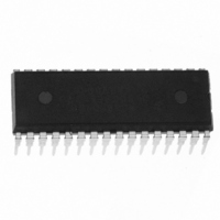
IC MCU 8K FLASH 8MHZ 32-DIP
Manufacturer
Freescale Semiconductor
Series
HC08r
Specifications of MC68HC908JL8CSPE
Core Processor
HC08
Core Size
8-Bit
Speed
8MHz
Connectivity
SCI
Peripherals
LED, LVD, POR, PWM
Number Of I /o
26
Program Memory Size
8KB (8K x 8)
Program Memory Type
FLASH
Ram Size
256 x 8
Voltage - Supply (vcc/vdd)
2.7 V ~ 5.5 V
Data Converters
A/D 13x8b
Oscillator Type
Internal
Operating Temperature
-40°C ~ 85°C
Package / Case
32-SDIP (0.400", 10.16mm)
Controller Family/series
HC08
No. Of I/o's
26
Ram Memory Size
256Byte
Cpu Speed
8MHz
No. Of Timers
2
Embedded Interface Type
I2C, SCI, SPI
Rohs Compliant
Yes
Processor Series
HC08JL
Core
HC08
Data Bus Width
8 bit
Data Ram Size
256 B
Interface Type
SCI
Maximum Clock Frequency
8 MHz
Number Of Programmable I/os
26
Number Of Timers
4
Operating Supply Voltage
0 V to 5 V
Maximum Operating Temperature
+ 125 C
Mounting Style
Through Hole
Development Tools By Supplier
FSICEBASE, DEMO908JL16E, M68CBL05CE
Minimum Operating Temperature
- 40 C
On-chip Adc
8 bit, 13 Channel
Lead Free Status / RoHS Status
Lead free / RoHS Compliant
Eeprom Size
-
Lead Free Status / Rohs Status
Details
Available stocks
Company
Part Number
Manufacturer
Quantity
Price
Company:

Part Number:
MC68HC908JL8CSPE
Manufacturer:
SINOPOWER
Quantity:
24 000
Company:
Part Number:
MC68HC908JL8CSPE
Manufacturer:
Freescale Semiconductor
Quantity:
135
Company:
Part Number:
MC68HC908JL8CSPE
Manufacturer:
FREESCALE
Quantity:
51
Part Number:
MC68HC908JL8CSPE
Manufacturer:
FREESCALE
Quantity:
20 000


Analog-to-Digital Converter (ADC)
10.3.1 ADC Port I/O Pins
PTB0–PTB7 and PTD0–PTD3 are general-purpose I/O pins that are shared with the ADC channels. The
channel select bits (ADC status and control register, $003C), define which ADC channel/port pin will be
used as the input signal. The ADC overrides the port I/O logic by forcing that pin as input to the ADC. The
remaining ADC channels/port pins are controlled by the port I/O logic and can be used as
general-purpose I/O. Writes to the port register or DDR will not have any affect on the port pin that is
selected by the ADC. Read of a port pin which is in use by the ADC will return a logic 0 if the corresponding
DDR bit is at logic 0. If the DDR bit is at logic 1, the value in the port data latch is read.
146
INTERNAL
DATA BUS
AIEN
INTERRUPT
LOGIC
READ DDRB/DDRD
WRITE DDRB/DDRD
WRITE PTB/PTD
READ PTB/PTD
COCO
BUS CLOCK
MC68HC908JL8/JK8 • MC68HC08JL8/JK8 • MC68HC908KL8 Data Sheet, Rev. 3.1
CONVERSION
COMPLETE
RESET
ADC DATA REGISTER
Figure 10-2. ADC Block Diagram
GENERATOR
ADIV[2:0]
CLOCK
ADC
ADC CLOCK
DDRBx/DDRDx
PTBx/PTDx
ADC VOLTAGE IN
ADCVIN
DISABLE
DISABLE
(1 OF 13 CHANNELS)
ADC0–ADC11
CHANNEL
SELECT
ADC CHANNEL x
ADCx
Freescale Semiconductor
ADC12
ADCH[4:0]
Related parts for MC68HC908JL8CSPE
Image
Part Number
Description
Manufacturer
Datasheet
Request
R

Part Number:
Description:
Manufacturer:
Freescale Semiconductor, Inc
Datasheet:
Part Number:
Description:
Manufacturer:
Freescale Semiconductor, Inc
Datasheet:
Part Number:
Description:
Manufacturer:
Freescale Semiconductor, Inc
Datasheet:
Part Number:
Description:
Manufacturer:
Freescale Semiconductor, Inc
Datasheet:
Part Number:
Description:
Manufacturer:
Freescale Semiconductor, Inc
Datasheet:
Part Number:
Description:
Manufacturer:
Freescale Semiconductor, Inc
Datasheet:
Part Number:
Description:
Manufacturer:
Freescale Semiconductor, Inc
Datasheet:
Part Number:
Description:
Manufacturer:
Freescale Semiconductor, Inc
Datasheet:
Part Number:
Description:
Manufacturer:
Freescale Semiconductor, Inc
Datasheet:
Part Number:
Description:
Manufacturer:
Freescale Semiconductor, Inc
Datasheet:
Part Number:
Description:
Manufacturer:
Freescale Semiconductor, Inc
Datasheet:
Part Number:
Description:
Manufacturer:
Freescale Semiconductor, Inc
Datasheet:
Part Number:
Description:
Manufacturer:
Freescale Semiconductor, Inc
Datasheet:
Part Number:
Description:
Manufacturer:
Freescale Semiconductor, Inc
Datasheet:
Part Number:
Description:
Manufacturer:
Freescale Semiconductor, Inc
Datasheet: