MC9S08AW60CPUE Freescale Semiconductor, MC9S08AW60CPUE Datasheet - Page 11
MC9S08AW60CPUE
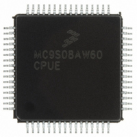
Manufacturer Part Number
MC9S08AW60CPUE
Description
IC MCU 64K FLASH 64-LQFP
Manufacturer
Freescale Semiconductor
Series
HCS08r
Datasheet
1.MC9S08AW32CFDE.pdf
(324 pages)
Specifications of MC9S08AW60CPUE
Core Processor
HCS08
Core Size
8-Bit
Speed
40MHz
Connectivity
I²C, SCI, SPI
Peripherals
LVD, POR, PWM, WDT
Number Of I /o
54
Program Memory Size
60KB (60K x 8)
Program Memory Type
FLASH
Ram Size
2K x 8
Voltage - Supply (vcc/vdd)
2.7 V ~ 5.5 V
Data Converters
A/D 16x10b
Oscillator Type
Internal
Operating Temperature
-40°C ~ 85°C
Package / Case
64-LQFP
Processor Series
S08AW
Core
HCS08
Data Bus Width
8 bit
Data Ram Size
2 KB
Interface Type
SCI/SPI
Maximum Clock Frequency
40 MHz
Number Of Programmable I/os
54
Number Of Timers
8
Operating Supply Voltage
- 0.3 V to + 5.8 V
Maximum Operating Temperature
+ 85 C
Mounting Style
SMD/SMT
3rd Party Development Tools
EWS08
Development Tools By Supplier
DEMO9S08AW60E
Minimum Operating Temperature
- 40 C
On-chip Adc
16-ch x 10-bit
For Use With
DEMO9S08AW60E - DEMO BOARD FOR MC9S08AW60
Lead Free Status / RoHS Status
Lead free / RoHS Compliant
Eeprom Size
-
Lead Free Status / Rohs Status
Lead free / RoHS Compliant
Available stocks
Company
Part Number
Manufacturer
Quantity
Price
Company:

Part Number:
MC9S08AW60CPUE
Manufacturer:
TDK-LAMBDA
Quantity:
92
Company:
Part Number:
MC9S08AW60CPUE
Manufacturer:
FREESCALE
Quantity:
4 000
Company:
Part Number:
MC9S08AW60CPUE
Manufacturer:
Freescale Semiconductor
Quantity:
10 000
Part Number:
MC9S08AW60CPUE
Manufacturer:
FREESCALE
Quantity:
20 000
Company:
Part Number:
MC9S08AW60CPUER
Manufacturer:
Freescale Semiconductor
Quantity:
10 000


Section Number
6.1
6.2
6.3
6.4
6.5
6.6
6.7
7.1
7.2
Freescale Semiconductor
Introduction .....................................................................................................................................81
Features ...........................................................................................................................................81
Pin Descriptions ..............................................................................................................................82
Parallel I/O Control .........................................................................................................................86
Pin Control ......................................................................................................................................87
Pin Behavior in Stop Modes ............................................................................................................88
Parallel I/O and Pin Control Registers ............................................................................................88
Introduction ...................................................................................................................................109
Programmer’s Model and CPU Registers .....................................................................................110
5.9.8
5.9.9
6.3.1
6.3.2
6.3.3
6.3.4
6.3.5
6.3.6
6.3.7
6.5.1
6.5.2
6.5.3
6.7.1
6.7.2
6.7.3
6.7.4
6.7.5
6.7.6
6.7.7
6.7.8
6.7.9
6.7.10
6.7.11
6.7.12
6.7.13
6.7.14
7.1.1
System Power Management Status and Control 1 Register (SPMSC1) .........................79
System Power Management Status and Control 2 Register (SPMSC2) .........................80
Port A ..............................................................................................................................82
Port B ..............................................................................................................................82
Port C ..............................................................................................................................83
Port D ..............................................................................................................................83
Port E ..............................................................................................................................84
Port F ..............................................................................................................................85
Port G ..............................................................................................................................85
Internal Pullup Enable ....................................................................................................87
Output Slew Rate Control Enable ..................................................................................87
Output Drive Strength Select ..........................................................................................87
Port A I/O Registers (PTAD and PTADD) .....................................................................88
Port A Pin Control Registers (PTAPE, PTASE, PTADS) ..............................................89
Port B I/O Registers (PTBD and PTBDD) .....................................................................91
Port B Pin Control Registers (PTBPE, PTBSE, PTBDS) ..............................................92
Port C I/O Registers (PTCD and PTCDD) .....................................................................94
Port C Pin Control Registers (PTCPE, PTCSE, PTCDS) ..............................................95
Port D I/O Registers (PTDD and PTDDD) ....................................................................97
Port D Pin Control Registers (PTDPE, PTDSE, PTDDS) .............................................98
Port E I/O Registers (PTED and PTEDD) ....................................................................100
Port E Pin Control Registers (PTEPE, PTESE, PTEDS) .............................................101
Port F I/O Registers (PTFD and PTFDD) ....................................................................103
Port F Pin Control Registers (PTFPE, PTFSE, PTFDS) ..............................................104
Port G I/O Registers (PTGD and PTGDD) ..................................................................106
Port G Pin Control Registers (PTGPE, PTGSE, PTGDS) ...........................................107
Features .........................................................................................................................109
Central Processor Unit (S08CPUV2)
Parallel Input/Output
MC9S08AW60 Data Sheet, Rev 2
Chapter 6
Chapter 7
Title
Page
11
Related parts for MC9S08AW60CPUE
Image
Part Number
Description
Manufacturer
Datasheet
Request
R

Part Number:
Description:
Manufacturer:
Freescale Semiconductor, Inc
Datasheet:
Part Number:
Description:
Manufacturer:
Freescale Semiconductor, Inc
Datasheet:
Part Number:
Description:
Manufacturer:
Freescale Semiconductor, Inc
Datasheet:
Part Number:
Description:
Manufacturer:
Freescale Semiconductor, Inc
Datasheet:
Part Number:
Description:
Manufacturer:
Freescale Semiconductor, Inc
Datasheet:
Part Number:
Description:
Manufacturer:
Freescale Semiconductor, Inc
Datasheet:
Part Number:
Description:
Manufacturer:
Freescale Semiconductor, Inc
Datasheet:
Part Number:
Description:
Manufacturer:
Freescale Semiconductor, Inc
Datasheet:
Part Number:
Description:
Manufacturer:
Freescale Semiconductor, Inc
Datasheet:
Part Number:
Description:
Manufacturer:
Freescale Semiconductor, Inc
Datasheet:
Part Number:
Description:
Manufacturer:
Freescale Semiconductor, Inc
Datasheet:
Part Number:
Description:
Manufacturer:
Freescale Semiconductor, Inc
Datasheet:
Part Number:
Description:
Manufacturer:
Freescale Semiconductor, Inc
Datasheet:
Part Number:
Description:
Manufacturer:
Freescale Semiconductor, Inc
Datasheet:
Part Number:
Description:
Manufacturer:
Freescale Semiconductor, Inc
Datasheet: