MC9S08AW60CPUE Freescale Semiconductor, MC9S08AW60CPUE Datasheet - Page 17
MC9S08AW60CPUE
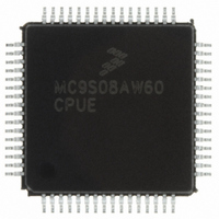
Manufacturer Part Number
MC9S08AW60CPUE
Description
IC MCU 64K FLASH 64-LQFP
Manufacturer
Freescale Semiconductor
Series
HCS08r
Datasheet
1.MC9S08AW32CFDE.pdf
(324 pages)
Specifications of MC9S08AW60CPUE
Core Processor
HCS08
Core Size
8-Bit
Speed
40MHz
Connectivity
I²C, SCI, SPI
Peripherals
LVD, POR, PWM, WDT
Number Of I /o
54
Program Memory Size
60KB (60K x 8)
Program Memory Type
FLASH
Ram Size
2K x 8
Voltage - Supply (vcc/vdd)
2.7 V ~ 5.5 V
Data Converters
A/D 16x10b
Oscillator Type
Internal
Operating Temperature
-40°C ~ 85°C
Package / Case
64-LQFP
Processor Series
S08AW
Core
HCS08
Data Bus Width
8 bit
Data Ram Size
2 KB
Interface Type
SCI/SPI
Maximum Clock Frequency
40 MHz
Number Of Programmable I/os
54
Number Of Timers
8
Operating Supply Voltage
- 0.3 V to + 5.8 V
Maximum Operating Temperature
+ 85 C
Mounting Style
SMD/SMT
3rd Party Development Tools
EWS08
Development Tools By Supplier
DEMO9S08AW60E
Minimum Operating Temperature
- 40 C
On-chip Adc
16-ch x 10-bit
For Use With
DEMO9S08AW60E - DEMO BOARD FOR MC9S08AW60
Lead Free Status / RoHS Status
Lead free / RoHS Compliant
Eeprom Size
-
Lead Free Status / Rohs Status
Lead free / RoHS Compliant
Available stocks
Company
Part Number
Manufacturer
Quantity
Price
Company:

Part Number:
MC9S08AW60CPUE
Manufacturer:
TDK-LAMBDA
Quantity:
92
Company:
Part Number:
MC9S08AW60CPUE
Manufacturer:
FREESCALE
Quantity:
4 000
Company:
Part Number:
MC9S08AW60CPUE
Manufacturer:
Freescale Semiconductor
Quantity:
10 000
Part Number:
MC9S08AW60CPUE
Manufacturer:
FREESCALE
Quantity:
20 000
Company:
Part Number:
MC9S08AW60CPUER
Manufacturer:
Freescale Semiconductor
Quantity:
10 000


Section Number
15.1 Introduction ...................................................................................................................................261
15.2 Background Debug Controller (BDC) ..........................................................................................262
15.3 On-Chip Debug System (DBG) ....................................................................................................271
15.4 Register Definition ........................................................................................................................275
A.1 Introduction ....................................................................................................................................283
A.2 Parameter Classification.................................................................................................................283
A.3 Absolute Maximum Ratings...........................................................................................................283
A.4 Thermal Characteristics..................................................................................................................285
A.5 ESD Protection and Latch-Up Immunity .......................................................................................286
A.6 DC Characteristics..........................................................................................................................287
A.7 Supply Current Characteristics.......................................................................................................291
A.8 ADC Characteristics.......................................................................................................................293
A.9 Internal Clock Generation Module Characteristics ........................................................................296
A.10 AC Characteristics..........................................................................................................................300
A.11 SPI Characteristics .........................................................................................................................303
A.12 FLASH Specifications....................................................................................................................306
A.13 EMC Performance..........................................................................................................................307
Freescale Semiconductor
15.1.1
15.2.1
15.2.2
15.2.3
15.2.4
15.3.1
15.3.2
15.3.3
15.3.4
15.3.5
15.3.6
15.4.1
15.4.2
15.4.3
A.9.1
A.10.1 Control Timing ..............................................................................................................300
A.10.2 Timer/PWM (TPM) Module Timing.............................................................................302
A.13.1 Radiated Emissions .......................................................................................................307
A.13.2 Conducted Transient Susceptibility...............................................................................307
Features .........................................................................................................................262
BKGD Pin Description .................................................................................................263
Communication Details ................................................................................................264
BDC Commands ...........................................................................................................268
BDC Hardware Breakpoint ..........................................................................................270
Comparators A and B ...................................................................................................271
Bus Capture Information and FIFO Operation .............................................................271
Change-of-Flow Information ........................................................................................272
Tag vs. Force Breakpoints and Triggers .......................................................................272
Trigger Modes ..............................................................................................................273
Hardware Breakpoints ..................................................................................................275
BDC Registers and Control Bits ...................................................................................275
System Background Debug Force Reset Register (SBDFR) ........................................277
DBG Registers and Control Bits ..................................................................................278
ICG Frequency Specifications.......................................................................................297
Electrical Characteristics and Timing Specifications
Development Support
MC9S08AW60 Data Sheet, Rev 2
Appendix A
Chapter 15
Title
Page
17
Related parts for MC9S08AW60CPUE
Image
Part Number
Description
Manufacturer
Datasheet
Request
R

Part Number:
Description:
Manufacturer:
Freescale Semiconductor, Inc
Datasheet:
Part Number:
Description:
Manufacturer:
Freescale Semiconductor, Inc
Datasheet:
Part Number:
Description:
Manufacturer:
Freescale Semiconductor, Inc
Datasheet:
Part Number:
Description:
Manufacturer:
Freescale Semiconductor, Inc
Datasheet:
Part Number:
Description:
Manufacturer:
Freescale Semiconductor, Inc
Datasheet:
Part Number:
Description:
Manufacturer:
Freescale Semiconductor, Inc
Datasheet:
Part Number:
Description:
Manufacturer:
Freescale Semiconductor, Inc
Datasheet:
Part Number:
Description:
Manufacturer:
Freescale Semiconductor, Inc
Datasheet:
Part Number:
Description:
Manufacturer:
Freescale Semiconductor, Inc
Datasheet:
Part Number:
Description:
Manufacturer:
Freescale Semiconductor, Inc
Datasheet:
Part Number:
Description:
Manufacturer:
Freescale Semiconductor, Inc
Datasheet:
Part Number:
Description:
Manufacturer:
Freescale Semiconductor, Inc
Datasheet:
Part Number:
Description:
Manufacturer:
Freescale Semiconductor, Inc
Datasheet:
Part Number:
Description:
Manufacturer:
Freescale Semiconductor, Inc
Datasheet:
Part Number:
Description:
Manufacturer:
Freescale Semiconductor, Inc
Datasheet: