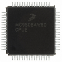
MC9S08AW60CPUE Freescale Semiconductor, MC9S08AW60CPUE Datasheet - Page 174

MC9S08AW60CPUE
Manufacturer Part Number
MC9S08AW60CPUE
Description
IC MCU 64K FLASH 64-LQFP
Manufacturer
Freescale Semiconductor
Series
HCS08r
Datasheet
1.MC9S08AW32CFDE.pdf
(324 pages)
Specifications of MC9S08AW60CPUE
Core Processor
HCS08
Core Size
8-Bit
Speed
40MHz
Connectivity
I²C, SCI, SPI
Peripherals
LVD, POR, PWM, WDT
Number Of I /o
54
Program Memory Size
60KB (60K x 8)
Program Memory Type
FLASH
Ram Size
2K x 8
Voltage - Supply (vcc/vdd)
2.7 V ~ 5.5 V
Data Converters
A/D 16x10b
Oscillator Type
Internal
Operating Temperature
-40°C ~ 85°C
Package / Case
64-LQFP
Processor Series
S08AW
Core
HCS08
Data Bus Width
8 bit
Data Ram Size
2 KB
Interface Type
SCI/SPI
Maximum Clock Frequency
40 MHz
Number Of Programmable I/os
54
Number Of Timers
8
Operating Supply Voltage
- 0.3 V to + 5.8 V
Maximum Operating Temperature
+ 85 C
Mounting Style
SMD/SMT
3rd Party Development Tools
EWS08
Development Tools By Supplier
DEMO9S08AW60E
Minimum Operating Temperature
- 40 C
On-chip Adc
16-ch x 10-bit
For Use With
DEMO9S08AW60E - DEMO BOARD FOR MC9S08AW60
Lead Free Status / RoHS Status
Lead free / RoHS Compliant
Eeprom Size
-
Lead Free Status / Rohs Status
Lead free / RoHS Compliant
Available stocks
Company
Part Number
Manufacturer
Quantity
Price
Company:
Part Number:
MC9S08AW60CPUE
Manufacturer:
TDK-LAMBDA
Quantity:
92
Company:
Part Number:
MC9S08AW60CPUE
Manufacturer:
FREESCALE
Quantity:
4 000
Company:
Part Number:
MC9S08AW60CPUE
Manufacturer:
Freescale Semiconductor
Quantity:
10 000
Part Number:
MC9S08AW60CPUE
Manufacturer:
FREESCALE
Quantity:
20 000
Company:
Part Number:
MC9S08AW60CPUER
Manufacturer:
Freescale Semiconductor
Quantity:
10 000
Chapter 10 Timer/Pulse-Width Modulator (S08TPMV2)
If the associated port pin is not stable for at least two bus clock cycles before changing to input capture
mode, it is possible to get an unexpected indication of an edge trigger. Typically, a program would clear
status flags after changing channel configuration bits and before enabling channel interrupts or using the
status flags to avoid any unexpected behavior.
10.4.5
These read/write registers contain the captured TPM counter value of the input capture function or the
output compare value for the output compare or PWM functions. The channel value registers are cleared
by reset.
In input capture mode, reading either byte (TPMxCnVH or TPMxCnVL) latches the contents of both bytes
into a buffer where they remain latched until the other byte is read. This latching mechanism also resets
(becomes unlatched) when the TPMxCnSC register is written.
174
CPWMS
Reset
Reset
X
0
1
W
W
R
R
Bit 15
Timer x Channel Value Registers (TPMxCnVH:TPMxCnVL)
Bit 7
0
0
7
7
MSnB:MSnA
XX
XX
1X
00
01
Figure 10-9. Timer x Channel Value Register High (TPMxCnVH)
Figure 10-10. Timer Channel Value Register Low (TPMxCnVL)
14
0
6
0
6
6
ELSnB:ELSnA
Table 10-5. Mode, Edge, and Level Selection
X1
X1
00
01
10
11
00
01
10
11
10
10
13
0
5
0
5
5
MC9S08AW60 Data Sheet, Rev 2
Pin not used for TPM channel; use as an external clock for the TPM or
revert to general-purpose I/O
Center-aligned
Input capture
Edge-aligned
compare
Output
12
Mode
PWM
PWM
0
4
0
4
4
Capture on rising edge only
Capture on falling edge only
Capture on rising or falling edge
Software compare only
Toggle output on compare
Clear output on compare
Set output on compare
High-true pulses (clear output on compare)
Low-true pulses (set output on compare)
High-true pulses (clear output on compare-up)
Low-true pulses (set output on compare-up)
11
3
0
3
3
0
10
0
2
0
2
2
Configuration
Freescale Semiconductor
9
0
1
0
1
1
Bit 8
Bit 0
0
0
0
0


