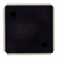
D6417729RHF200BV Renesas Electronics America, D6417729RHF200BV Datasheet - Page 200

D6417729RHF200BV
Manufacturer Part Number
D6417729RHF200BV
Description
IC SUPER H MPU ROMLESS 208QFP
Manufacturer
Renesas Electronics America
Series
SuperH® SH7700r
Datasheet
1.D6417729RF133BV.pdf
(857 pages)
Specifications of D6417729RHF200BV
Core Processor
SH-3 DSP
Core Size
32-Bit
Speed
200MHz
Connectivity
EBI/EMI, FIFO, IrDA, SCI, SmartCard
Peripherals
DMA, POR, WDT
Number Of I /o
96
Program Memory Type
ROMless
Ram Size
32K x 8
Voltage - Supply (vcc/vdd)
1.85 V ~ 2.15 V
Data Converters
A/D 8x10b; D/A 2x8b
Oscillator Type
Internal
Operating Temperature
-20°C ~ 75°C
Package / Case
208-QFP Exposed Pad, 208-eQFP, 208-HQFP
Lead Free Status / RoHS Status
Lead free / RoHS Compliant
Eeprom Size
-
Program Memory Size
-
Available stocks
Company
Part Number
Manufacturer
Quantity
Price
Company:
Part Number:
D6417729RHF200BV
Manufacturer:
EVERLIGHT
Quantity:
1 000
Company:
Part Number:
D6417729RHF200BV
Manufacturer:
Renesas Electronics America
Quantity:
10 000
- Current page: 200 of 857
- Download datasheet (5Mb)
and V bit specified in the data field are then written. Note that, when a 0 is written to the V bit, a 0
should always be written to the U bit of the same entry, too.
(3) Address Array Write (with Associative Operation)
The associative bit (A bit) in the address field indicates whether the addresses are compared
during writing. With the A bit set to 1, all 4 ways for the entry specified in the address field will be
compared to the tag address specified in the data field for a match. The values of the U bit and V
bit specified in the data field will be written to the way that has a hit. However, the tag address and
the LRU will not be changed. If no way receives a hit, writing does not take place and the result is
no operation.
This operation is used to invalidate the address specification for a cache. Write back will take
place when the U bit of the entry that received a hit is 1. Note that, when a 0 is written to the V bit,
a 0 should always be written to the U bit of the same entry, too.
5.4.2
Data Array
The address array is mapped to H'F1000000 to H'F1FFFFFF. To access an element of the data
array, the 32-bit address field (for read/write access) and 32-bit data field (for write access) must
be specified. The address field specifies the information that selects the entry to be accessed; the
data field specifies the longword data to be written to the data array.
In the address field, specify the entry's address in bits 11-4, L in bits 3-2 to indicate the longword's
position within a line (which consists of 16 bytes), W in bits 13-12 to select the way, and H'F1 in
bits 31-24 to indicate access to the data array. The L bits (3-2) specification is in the following
form: 00 is longword 0, 01 is longword 1, 10 is longword 2, and 11 is longword 3. Settings for the
W bits (13-12) are as follows: 00 is way 0, 01 is way 1, 10 is way 2, and 11 is way 3. Since access
is not allowed crossing longword boundaries, always set 00 in bits 1-0 of the address field.
The following two operations on the data array are possible. Note that these operations will not
change the information in the address array.
(1) Data Array Read
Reads the data at the position selected by the L bits (3-2) of the address field from the entry that
corresponds to the entry address and way that were specified in the address field.
(2) Data Array Write
Writes the longword data set in the data field into the entry that corresponds to the entry address
and way that were specified in the address field. The longword data will be written to the entry at
the position selected by the L bits (3-2) of the address field.
Rev. 5.0, 09/03, page 152 of 806
Related parts for D6417729RHF200BV
Image
Part Number
Description
Manufacturer
Datasheet
Request
R

Part Number:
Description:
KIT STARTER FOR M16C/29
Manufacturer:
Renesas Electronics America
Datasheet:

Part Number:
Description:
KIT STARTER FOR R8C/2D
Manufacturer:
Renesas Electronics America
Datasheet:

Part Number:
Description:
R0K33062P STARTER KIT
Manufacturer:
Renesas Electronics America
Datasheet:

Part Number:
Description:
KIT STARTER FOR R8C/23 E8A
Manufacturer:
Renesas Electronics America
Datasheet:

Part Number:
Description:
KIT STARTER FOR R8C/25
Manufacturer:
Renesas Electronics America
Datasheet:

Part Number:
Description:
KIT STARTER H8S2456 SHARPE DSPLY
Manufacturer:
Renesas Electronics America
Datasheet:

Part Number:
Description:
KIT STARTER FOR R8C38C
Manufacturer:
Renesas Electronics America
Datasheet:

Part Number:
Description:
KIT STARTER FOR R8C35C
Manufacturer:
Renesas Electronics America
Datasheet:

Part Number:
Description:
KIT STARTER FOR R8CL3AC+LCD APPS
Manufacturer:
Renesas Electronics America
Datasheet:

Part Number:
Description:
KIT STARTER FOR RX610
Manufacturer:
Renesas Electronics America
Datasheet:

Part Number:
Description:
KIT STARTER FOR R32C/118
Manufacturer:
Renesas Electronics America
Datasheet:

Part Number:
Description:
KIT DEV RSK-R8C/26-29
Manufacturer:
Renesas Electronics America
Datasheet:

Part Number:
Description:
KIT STARTER FOR SH7124
Manufacturer:
Renesas Electronics America
Datasheet:

Part Number:
Description:
KIT STARTER FOR H8SX/1622
Manufacturer:
Renesas Electronics America
Datasheet:

Part Number:
Description:
KIT DEV FOR SH7203
Manufacturer:
Renesas Electronics America
Datasheet:


