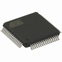
AT32UC3B0512-A2UT Atmel, AT32UC3B0512-A2UT Datasheet - Page 220

AT32UC3B0512-A2UT
Manufacturer Part Number
AT32UC3B0512-A2UT
Description
IC MCU AVR32 512K FLASH 64TQFP
Manufacturer
Atmel
Series
AVR®32 UC3r
Specifications of AT32UC3B0512-A2UT
Core Processor
AVR
Core Size
32-Bit
Speed
60MHz
Connectivity
I²C, IrDA, SPI, SSC, UART/USART, USB
Peripherals
Brown-out Detect/Reset, DMA, POR, PWM, WDT
Number Of I /o
44
Program Memory Size
512KB (512K x 8)
Program Memory Type
FLASH
Ram Size
96K x 8
Voltage - Supply (vcc/vdd)
1.65 V ~ 1.95 V
Data Converters
A/D 8x10b
Oscillator Type
Internal
Operating Temperature
-40°C ~ 85°C
Package / Case
64-TQFP, 64-VQFP
Controller Family/series
AT32UC3B
No. Of I/o's
44
Ram Memory Size
96KB
Cpu Speed
60MHz
No. Of Timers
1
Rohs Compliant
Yes
Lead Free Status / RoHS Status
Lead free / RoHS Compliant
Eeprom Size
-
Available stocks
Company
Part Number
Manufacturer
Quantity
Price
Company:
Part Number:
AT32UC3B0512-A2UT
Manufacturer:
MURATA
Quantity:
11 450
Part Number:
AT32UC3B0512-A2UT
Manufacturer:
ATMEL/爱特梅尔
Quantity:
20 000
- Current page: 220 of 692
- Download datasheet (11Mb)
19.5
Figure 19-2. Application Block Diagram
19.6
Table 19-3.
19.7
19.7.1
19.7.2
32059K–03/2011
Pin Name
TWD
TWCK
Application Block Diagram
I/O Lines Description
Product Dependencies
I/O Lines
Power Management
I/O Lines Description
Rp: Pull up value as given by the I²C Standard
Host with
Interface
TWI
Both TWD and TWCK are bidirectional lines, connected to a positive supply voltage via a current
source or pull-up resistor (see
high. The output stages of devices connected to the bus must have an open-drain or open-col-
lector to perform the wired-AND function.
TWD and TWCK pins may be multiplexed with GPIO lines. To enable the TWI, the programmer
must perform the following steps:
The TWI clock is generated by the Power Manager (PM). Before using the TWI, the programmer
must ensure that the TWI clock is enabled in the PM.
In the TWI description, Master Clock (MCK) is the clock of the peripheral bus to which the TWI is
connected.
TWD
TWCK
• Program the GPIO controller to:
Serial EEPROM
– Dedicate TWD and TWCK as peripheral lines.
– Define TWD and TWCK as open-drain.
Pin Description
Two-wire Serial Data
Two-wire Serial Clock
Atmel TWI
Slave 1
I²C RTC
Slave 2
Figure 19-2 on page
Controller
I²C LCD
Slave 3
I²C Temp.
220). When the bus is free, both lines are
Slave 4
Sensor
Rp
Rp
AT32UC3B
VDD
Input/Output
Input/Output
Type
220
Related parts for AT32UC3B0512-A2UT
Image
Part Number
Description
Manufacturer
Datasheet
Request
R

Part Number:
Description:
DEV KIT FOR AVR/AVR32
Manufacturer:
Atmel
Datasheet:

Part Number:
Description:
INTERVAL AND WIPE/WASH WIPER CONTROL IC WITH DELAY
Manufacturer:
ATMEL Corporation
Datasheet:

Part Number:
Description:
Low-Voltage Voice-Switched IC for Hands-Free Operation
Manufacturer:
ATMEL Corporation
Datasheet:

Part Number:
Description:
MONOLITHIC INTEGRATED FEATUREPHONE CIRCUIT
Manufacturer:
ATMEL Corporation
Datasheet:

Part Number:
Description:
AM-FM Receiver IC U4255BM-M
Manufacturer:
ATMEL Corporation
Datasheet:

Part Number:
Description:
Monolithic Integrated Feature Phone Circuit
Manufacturer:
ATMEL Corporation
Datasheet:

Part Number:
Description:
Multistandard Video-IF and Quasi Parallel Sound Processing
Manufacturer:
ATMEL Corporation
Datasheet:

Part Number:
Description:
High-performance EE PLD
Manufacturer:
ATMEL Corporation
Datasheet:

Part Number:
Description:
8-bit Flash Microcontroller
Manufacturer:
ATMEL Corporation
Datasheet:

Part Number:
Description:
2-Wire Serial EEPROM
Manufacturer:
ATMEL Corporation
Datasheet:


