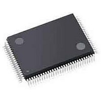
A3PN125-ZVQG100 Actel, A3PN125-ZVQG100 Datasheet - Page 17

A3PN125-ZVQG100
Manufacturer Part Number
A3PN125-ZVQG100
Description
FPGA - Field Programmable Gate Array 125K System Gates ProASIC3 nano
Manufacturer
Actel
Datasheet
1.A3PN030-ZVQG100.pdf
(106 pages)
Specifications of A3PN125-ZVQG100
Processor Series
A3PN125
Core
IP Core
Number Of Macrocells
1024
Maximum Operating Frequency
350 MHz
Number Of Programmable I/os
71
Data Ram Size
36 Kbit
Delay Time
1.02 ns
Supply Voltage (max)
3.3 V
Supply Current
2 mA
Maximum Operating Temperature
+ 70 C
Minimum Operating Temperature
- 20 C
Development Tools By Supplier
AGLN-Nano-Kit, AGLN-Z-Nano-Kit, Silicon-Explorer II, Silicon-Sculptor 3, SI-EX-TCA, FloasPro 4, FlashPro 3, FlashPro Lite
Mounting Style
SMD/SMT
Supply Voltage (min)
1.5 V
Number Of Gates
125 K
Package / Case
VQFP-100
Lead Free Status / RoHS Status
Lead free / RoHS Compliant
Available stocks
Company
Part Number
Manufacturer
Quantity
Price
Company:
Part Number:
A3PN125-ZVQG100
Manufacturer:
Microsemi SoC
Quantity:
10 000
Company:
Part Number:
A3PN125-ZVQG100I
Manufacturer:
Microsemi SoC
Quantity:
10 000
Table 2-4 • Overshoot and Undershoot Limits
VCCI and VMV
2.7 V or less
3 V
3.3 V
3.6 V
Notes:
1. Based on reliability requirements at 85°C.
2. The duration is allowed at one out of six clock cycles. If the overshoot/undershoot occurs at one out of two cycles, the
maximum overshoot/undershoot has to be reduced by 0.15 V.
I/O Power-Up and Supply Voltage Thresholds for Power-On Reset
(Commercial and Industrial)
Sophisticated power-up management circuitry is designed into every ProASIC
ensure easy transition from the powered-off state to the powered-up state of the device. The many
different supplies can power up in any sequence with minimized current spikes or surges. In addition, the
I/O will be in a known state through the power-up sequence. The basic principle is shown in
on page
There are five regions to consider during power-up.
ProASIC3 I/Os are activated only if ALL of the following three conditions are met:
VCCI Trip Point:
Ramping up: 0.6 V < trip_point_up < 1.2 V
Ramping down: 0.5 V < trip_point_down < 1.1 V
VCC Trip Point:
Ramping up: 0.6 V < trip_point_up < 1.1 V
Ramping down: 0.5 V < trip_point_down < 1 V
VCC and VCCI ramp-up trip points are about 100 mV higher than ramp-down trip points. This specifically
built-in hysteresis prevents undesirable power-up oscillations and current surges. Note the following:
PLL Behavior at Brownout Condition
Actel recommends using monotonic power supplies or voltage regulators to ensure proper power-up
behavior. Power ramp-up should be monotonic at least until VCC and VCCPLLX exceed brownout
activation levels. The VCC activation level is specified as 1.1 V worst-case (see
for more details).
When PLL power supply voltage and/or VCC levels drop below the VCC brownout levels (0.75 V ±
0.25 V), the PLL output lock signal goes low and/or the output clock is lost. Refer to the
"Power-Up/-Down Behavior of Low Power Flash Devices" chapter of the
User’s Guide
1. VCC and VCCI are above the minimum specified trip points
2. VCCI > VCC – 0.75 V (typical)
3. Chip is in the operating mode.
•
•
During programming, I/Os become tristated and weakly pulled up to VCCI.
JTAG supply, PLL power supplies, and charge pump VPUMP supply have no influence on I/O
behavior.
2-4.
for information on clock and lock recovery.
Average VCCI–GND Overshoot or Undershoot
Duration as a Percentage of Clock Cycle
1
10%
10%
10%
10%
5%
5%
5%
5%
R e v i s i o n 8
2
(Figure 2-1 on page
ProASIC3 nano FPGA Fabric
Maximum Overshoot/
ProASIC3 nano Flash FPGAs
®
3 device. These circuits
Undershoot
Figure 2-1 on page 2-4
1.49 V
1.19 V
0.79 V
0.88 V
0.45 V
0.54 V
1.4 V
1.1 V
2-4).
Figure 2-1
2
2 -3


