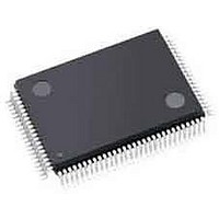
A3PN125-ZVQG100 Actel, A3PN125-ZVQG100 Datasheet - Page 18

A3PN125-ZVQG100
Manufacturer Part Number
A3PN125-ZVQG100
Description
FPGA - Field Programmable Gate Array 125K System Gates ProASIC3 nano
Manufacturer
Actel
Datasheet
1.A3PN030-ZVQG100.pdf
(106 pages)
Specifications of A3PN125-ZVQG100
Processor Series
A3PN125
Core
IP Core
Number Of Macrocells
1024
Maximum Operating Frequency
350 MHz
Number Of Programmable I/os
71
Data Ram Size
36 Kbit
Delay Time
1.02 ns
Supply Voltage (max)
3.3 V
Supply Current
2 mA
Maximum Operating Temperature
+ 70 C
Minimum Operating Temperature
- 20 C
Development Tools By Supplier
AGLN-Nano-Kit, AGLN-Z-Nano-Kit, Silicon-Explorer II, Silicon-Sculptor 3, SI-EX-TCA, FloasPro 4, FlashPro 3, FlashPro Lite
Mounting Style
SMD/SMT
Supply Voltage (min)
1.5 V
Number Of Gates
125 K
Package / Case
VQFP-100
Lead Free Status / RoHS Status
Lead free / RoHS Compliant
Available stocks
Company
Part Number
Manufacturer
Quantity
Price
Company:
Part Number:
A3PN125-ZVQG100
Manufacturer:
Microsemi SoC
Quantity:
10 000
Company:
Part Number:
A3PN125-ZVQG100I
Manufacturer:
Microsemi SoC
Quantity:
10 000
ProASIC3 nano DC and Switching Characteristics
Figure 2-1 • I/O State as a Function of VCCI and VCC Voltage Levels
2 - 4
Deactivation trip point:
Activation trip point:
V
V
d
a
= 0.85 V ± 0.25 V
= 0.75 V ± 0.25 V
VCC = 1.575 V
VCC = 1.425 V
Internal Power-Up Activation Sequence
1. Core
2. Input buffers
3. Output buffers, after 200 ns delay from input buffer activation
VCC
Region 1: I/O Buffers are OFF
Deactivation trip point:
VCC = VCCI + VT
where VT can be from 0.58 V to 0.9 V (typically 0.75 V)
Activation trip point:
V
V
a
d
= 0.9 V ± 0.3 V
= 0.8 V ± 0.3 V
Region 1: I/O buffers are OFF
Region 2: I/O buffers are ON.
I/Os are functional but slower because
VCCI / VCC are below specification.
For the same reason, input
buffers do not meet VIH / VIL levels, and
output buffers do not meet VOH / VOL levels.
buffers do not meet VOH/VOL levels.
not meet VIH / VIL levels, and output
same reason, input buffers do
is below specification. For the
but slower because VCCI
I/Os are functional
R e vi s i o n 8
buffers are ON.
Region 4: I/O
Min
standard; i.e., 1.425 V or 1.7 V
voltage at a selected I/O
VCCI
or 2.3 V or 3.0 V
datasheet specification
speed, VIH / VIL , VOH / VOL , etc.
Region 3: I/O buffers are ON.
I/Os are functional; I/O DC
specifications are met,
but I/Os are slower because
the VCC is below specification.
Region 5: I/O buffers are ON
and power supplies are within
specification.
I/Os meet the entire datasheet
and timer specifications for
VCCI


