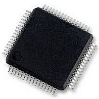
HD64F36077GHV Renesas Electronics America, HD64F36077GHV Datasheet - Page 22

HD64F36077GHV
Manufacturer Part Number
HD64F36077GHV
Description
16BIT MCU FLASH 56K, SMD, LQFP64
Manufacturer
Renesas Electronics America
Datasheet
1.HD64F36077GHV.pdf
(524 pages)
Specifications of HD64F36077GHV
No. Of I/o's
47
Ram Memory Size
4KB
Cpu Speed
20MHz
No. Of Timers
4
Digital Ic Case Style
LQFP
Supply Voltage Range
4.5V
Core Size
16bit
Program Memory Size
56KB
Oscillator Type
External Only
Controller Family/series
H8/300H
Peripherals
ADC
Rohs Compliant
Yes
Lead Free Status / RoHS Status
Lead free / RoHS Compliant
Available stocks
Company
Part Number
Manufacturer
Quantity
Price
Company:
Part Number:
HD64F36077GHV
Manufacturer:
RENESAS
Quantity:
340
Part Number:
HD64F36077GHV
Manufacturer:
RENESAS/瑞萨
Quantity:
20 000
- Current page: 22 of 524
- Download datasheet (4Mb)
Figure 13.22 Example of PWM Mode Operation (1) ................................................................. 228
Figure 13.23 Example of PWM Mode Operation (2) ................................................................. 229
Figure 13.24 Example of PWM Mode Operation (3) ................................................................. 230
Figure 13.25 Example of PWM Mode Operation (4) ................................................................. 231
Figure 13.26 Example of Reset Synchronous PWM Mode Setting Procedure........................... 233
Figure 13.27 Example of Reset Synchronous PWM Mode Operation (OLS0 = OLS1 = 1) ...... 234
Figure 13.28 Example of Reset Synchronous PWM Mode Operation (OLS0 = OLS1 = 0) ...... 235
Figure 13.29 Example of Complementary PWM Mode Setting Procedure................................ 237
Figure 13.30 Canceling Procedure of Complementary PWM Mode.......................................... 238
Figure 13.31 Example of Complementary PWM Mode Operation (1) ...................................... 239
Figure 13.32 (1) Example of Complementary PWM Mode Operation
Figure 13.32 (2) Example of Complementary PWM Mode Operation
Figure 13.33 Timing of Overshooting ........................................................................................ 243
Figure 13.34 Timing of Undershooting ...................................................................................... 243
Figure 13.35 Compare Match Buffer Operation......................................................................... 246
Figure 13.36 Input Capture Buffer Operation............................................................................. 247
Figure 13.37 Example of Buffer Operation Setting Procedure................................................... 247
Figure 13.38 Example of Buffer Operation (1)
Figure 13.39 Example of Compare Match Timing for Buffer Operation ................................... 249
Figure 13.40 Example of Buffer Operation (2)
Figure 13.41 Input Capture Timing of Buffer Operation............................................................ 251
Figure 13.42 Buffer Operation (3)
Figure 13.43 Buffer Operation (4)
Figure 13.44 Example of Output Disable Timing of Timer Z by Writing to TOER .................. 254
Figure 13.45 Example of Output Disable Timing of Timer Z by External Trigger.................... 255
Figure 13.46 Example of Output Inverse Timing of Timer Z by Writing to TFCR ................... 256
Figure 13.47 Example of Output Inverse Timing of Timer Z by Writing to POCR................... 256
Figure 13.48 IMF Flag Set Timing when Compare Match Occurs ............................................ 257
Figure 13.49 IMF Flag Set Timing at Input Capture .................................................................. 258
Figure 13.50 OVF Flag Set Timing ............................................................................................ 258
Figure 13.51 Status Flag Clearing Timing.................................................................................. 259
Figure 13.52 Contention between TCNT Write and Clear Operations....................................... 260
Figure 13.53 Contention between TCNT Write and Increment Operations ............................... 261
Figure 13.54 Contention between GR Write and Compare Match............................................. 261
Rev. 1.00 Sep. 16, 2005 Page xxii of xxx
(TPSC2 = TPSC1 = TPSC0 = 0) (2)...................................................................... 241
(TPSC2 = TPSC1 = TPSC0 ≠ 0) (3)...................................................................... 242
(Buffer Operation for Output Compare Register).................................................. 248
(Buffer Operation for Input Capture Register) ...................................................... 250
(Buffer Operation in Complementary PWM Mode CMD1 = CMD0 = 1) ............ 252
(Buffer Operation in Complementary PWM Mode CMD1 = CMD0 = 1) ............ 253
Related parts for HD64F36077GHV
Image
Part Number
Description
Manufacturer
Datasheet
Request
R

Part Number:
Description:
KIT STARTER FOR M16C/29
Manufacturer:
Renesas Electronics America
Datasheet:

Part Number:
Description:
KIT STARTER FOR R8C/2D
Manufacturer:
Renesas Electronics America
Datasheet:

Part Number:
Description:
R0K33062P STARTER KIT
Manufacturer:
Renesas Electronics America
Datasheet:

Part Number:
Description:
KIT STARTER FOR R8C/23 E8A
Manufacturer:
Renesas Electronics America
Datasheet:

Part Number:
Description:
KIT STARTER FOR R8C/25
Manufacturer:
Renesas Electronics America
Datasheet:

Part Number:
Description:
KIT STARTER H8S2456 SHARPE DSPLY
Manufacturer:
Renesas Electronics America
Datasheet:

Part Number:
Description:
KIT STARTER FOR R8C38C
Manufacturer:
Renesas Electronics America
Datasheet:

Part Number:
Description:
KIT STARTER FOR R8C35C
Manufacturer:
Renesas Electronics America
Datasheet:

Part Number:
Description:
KIT STARTER FOR R8CL3AC+LCD APPS
Manufacturer:
Renesas Electronics America
Datasheet:

Part Number:
Description:
KIT STARTER FOR RX610
Manufacturer:
Renesas Electronics America
Datasheet:

Part Number:
Description:
KIT STARTER FOR R32C/118
Manufacturer:
Renesas Electronics America
Datasheet:

Part Number:
Description:
KIT DEV RSK-R8C/26-29
Manufacturer:
Renesas Electronics America
Datasheet:

Part Number:
Description:
KIT STARTER FOR SH7124
Manufacturer:
Renesas Electronics America
Datasheet:

Part Number:
Description:
KIT STARTER FOR H8SX/1622
Manufacturer:
Renesas Electronics America
Datasheet:


