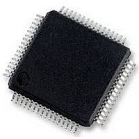
HD64F36077GHV Renesas Electronics America, HD64F36077GHV Datasheet - Page 296

HD64F36077GHV
Manufacturer Part Number
HD64F36077GHV
Description
16BIT MCU FLASH 56K, SMD, LQFP64
Manufacturer
Renesas Electronics America
Datasheet
1.HD64F36077GHV.pdf
(524 pages)
Specifications of HD64F36077GHV
No. Of I/o's
47
Ram Memory Size
4KB
Cpu Speed
20MHz
No. Of Timers
4
Digital Ic Case Style
LQFP
Supply Voltage Range
4.5V
Core Size
16bit
Program Memory Size
56KB
Oscillator Type
External Only
Controller Family/series
H8/300H
Peripherals
ADC
Rohs Compliant
Yes
Lead Free Status / RoHS Status
Lead free / RoHS Compliant
Available stocks
Company
Part Number
Manufacturer
Quantity
Price
Company:
Part Number:
HD64F36077GHV
Manufacturer:
RENESAS
Quantity:
340
Part Number:
HD64F36077GHV
Manufacturer:
RENESAS/瑞萨
Quantity:
20 000
- Current page: 296 of 524
- Download datasheet (4Mb)
Section 13 Timer Z
9. Note on Writing to the TOA0 to TOD0 Bits and the TOA1 to TOD1 Bits in TOCR:
BCLR#2, @TOCR
Rev. 1.00 Sep. 16, 2005 Page 266 of 490
REJ09B0216-0100
(1) TOCR read operation: Read H'06
(2) Modify operation: Modify H'06 to H'02
(3) Write operation to TOCR: Write H'02
TOCR
write signal
Compare match
signal B0
FTIOB0 pin
TOCR has been set to H'06. Compare match B0 and compare match C0 are used. The FTIOB0 pin is in the 1 output state,
and is set to the toggle output or the 0 output by compare match B0.
When BCLR#2, @TOCR is executed to clear the TOC0 bit (the FTIOC0 signal is low) and compare match B0 occurs
at the same timing as shown below, the H'02 writing to TOCR has priority and compare match B0 does not drive the FTIOB0 signal low;
the FTIOB0 signal remains high.
Bit
TOCR
Set value
The TOA0 to TOD0 bits and the TOA1 to TOD1 bits in TOCR decide the value of the FTIO
pin, which is output until the first compare match occurs. Once a compare match occurs and
this compare match changes the values of FTIOA0 to FTIOD0 and FTIOA1 to FTIOD1
output, the values of the FTIOA0 to FTIOD0 and FTIOA1 to FTIOD1 pin output and the
values read from the TOA0 to TOD0 and TOA1 to TOD1 bits may differ. Moreover, when the
writing to TOCR and the generation of the compare match A0 to D0 and A1 to D1 occur at the
same timing, the writing to TOCR has the priority. Thus, output change due to the compare
match is not reflected to the FTIOA0 to FTIOD0 and FTIOA1 to FTIOD1 pins. Therefore,
when bit manipulation instruction is used to write to TOCR, the values of the FTIOA0 to
FTIOD0 and FTIOA1 to FTIOD1 pin output may result in an unexpected result. When TOCR
is to be written to while compare match is operating, stop the counter once before accessing to
TOCR, read the port 6 state to reflect the values of FTIOA0 to FTIOD0 and FTIOA1 to
FTIOD1 output, to TOA0 to TOD0 and TOA1 to TOD1, and then restart the counter. Figure
13.59 shows an example when the compare match and the bit manipulation instruction to
TOCR occur at the same timing.
φ
Figure 13.59 When Compare Match and Bit Manipulation Instruction to TOCR
TOD1
7
0
TOC1
6
0
TOB1
5
0
Occur at the Same Timing
TOA1
4
0
TOD0
Remains high because the 1 writing to TOB has priority
3
0
TOC0
2
1
TOB0
1
1
TOA0
0
0
Expected output
Related parts for HD64F36077GHV
Image
Part Number
Description
Manufacturer
Datasheet
Request
R

Part Number:
Description:
KIT STARTER FOR M16C/29
Manufacturer:
Renesas Electronics America
Datasheet:

Part Number:
Description:
KIT STARTER FOR R8C/2D
Manufacturer:
Renesas Electronics America
Datasheet:

Part Number:
Description:
R0K33062P STARTER KIT
Manufacturer:
Renesas Electronics America
Datasheet:

Part Number:
Description:
KIT STARTER FOR R8C/23 E8A
Manufacturer:
Renesas Electronics America
Datasheet:

Part Number:
Description:
KIT STARTER FOR R8C/25
Manufacturer:
Renesas Electronics America
Datasheet:

Part Number:
Description:
KIT STARTER H8S2456 SHARPE DSPLY
Manufacturer:
Renesas Electronics America
Datasheet:

Part Number:
Description:
KIT STARTER FOR R8C38C
Manufacturer:
Renesas Electronics America
Datasheet:

Part Number:
Description:
KIT STARTER FOR R8C35C
Manufacturer:
Renesas Electronics America
Datasheet:

Part Number:
Description:
KIT STARTER FOR R8CL3AC+LCD APPS
Manufacturer:
Renesas Electronics America
Datasheet:

Part Number:
Description:
KIT STARTER FOR RX610
Manufacturer:
Renesas Electronics America
Datasheet:

Part Number:
Description:
KIT STARTER FOR R32C/118
Manufacturer:
Renesas Electronics America
Datasheet:

Part Number:
Description:
KIT DEV RSK-R8C/26-29
Manufacturer:
Renesas Electronics America
Datasheet:

Part Number:
Description:
KIT STARTER FOR SH7124
Manufacturer:
Renesas Electronics America
Datasheet:

Part Number:
Description:
KIT STARTER FOR H8SX/1622
Manufacturer:
Renesas Electronics America
Datasheet:


