PIC18C801-I/L Microchip Technology, PIC18C801-I/L Datasheet - Page 116
PIC18C801-I/L
Manufacturer Part Number
PIC18C801-I/L
Description
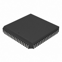
IC,MICROCONTROLLER,8-BIT,PIC CPU,CMOS,LDCC,84PIN,PLASTIC
Manufacturer
Microchip Technology
Series
PIC® 18Cr
Datasheets
1.PIC16F616T-ISL.pdf
(8 pages)
2.PIC18C601-IL.pdf
(320 pages)
3.PIC18C601-IL.pdf
(10 pages)
4.PIC18C601-IL.pdf
(10 pages)
Specifications of PIC18C801-I/L
Rohs Compliant
YES
Core Processor
PIC
Core Size
8-Bit
Speed
25MHz
Connectivity
EBI/EMI, I²C, SPI, UART/USART
Peripherals
Brown-out Detect/Reset, LVD, POR, PWM, WDT
Number Of I /o
37
Program Memory Type
ROMless
Ram Size
1.5K x 8
Voltage - Supply (vcc/vdd)
4.2 V ~ 5.5 V
Data Converters
A/D 12x10b
Oscillator Type
External
Operating Temperature
-40°C ~ 85°C
Package / Case
84-PLCC
Processor Series
PIC18C
Core
PIC
Data Bus Width
8 bit
Data Ram Size
1.5 KB
Interface Type
3-Wire, I2C, SPI, USART
Maximum Clock Frequency
25 MHz
Number Of Programmable I/os
47
Number Of Timers
1 x 16 bit
Operating Supply Voltage
2 V to 5.5 V
Maximum Operating Temperature
+ 85 C
Mounting Style
SMD/SMT
3rd Party Development Tools
52715-96, 52716-328, 52717-734, 52712-325, EWPIC18
Development Tools By Supplier
DV164005, ICE4000, DV164136
Minimum Operating Temperature
- 40 C
On-chip Adc
10 bit
Lead Free Status / RoHS Status
Lead free / RoHS Compliant
For Use With
AC164310 - MODULE SKT FOR PM3 84PLCCXLT84L1 - SOCKET TRANSITION ICE 84PLCCAC174012 - MODULE SKT PROMATEII 84PLCC
Eeprom Size
-
Program Memory Size
-
Lead Free Status / Rohs Status
Details
Other names
PIC18C801-I/LR
PIC18C801-I/LR
PIC18C801I/L
PIC18C801-I/LR
PIC18C801I/L
Available stocks
Company
Part Number
Manufacturer
Quantity
Price
Company:

Part Number:
PIC18C801-I/L
Manufacturer:
MICROCHIP
Quantity:
12 000
Company:
Part Number:
PIC18C801-I/L
Manufacturer:
Microchip Technology
Quantity:
10 000


PIC18C601/801
9.6
PORTF is an 8-bit wide, bi-directional port. The corre-
sponding data direction register is TRISF. Setting a
TRISF bit (= 1) will make the corresponding PORTF pin
an input (i.e., put the corresponding output driver in a
Hi-Impedance mode). Clearing a TRISF bit (= 0) will
make the corresponding PORTF pin an output (i.e., put
the contents of the output latch on the selected pin).
Read-modify-write operations on the LATF register
reads and writes the latched output value for PORTF.
PORTF pins, RF2:RF0, are multiplexed with analog
inputs. The operation of these pins are selected by
ADCON0 and ADCON1 registers.
PORTF pins, RF3 and RF5, are multiplexed with two of
the integrated chip select signals CSIO and CS1. For
PIC18C801, pin RF4 is multiplexed with chip select sig-
nal CS2, while for PIC18C601, it is multiplexed with
system bus signal A16. For PIC18C801 devices, both
CSEL2 and CSELIO registers must set to all zero, to
enable these pins as I/O pins, while for PIC18C601
devices, only CSELIO register needs to be set to zero.
For PIC18C601 devices, pin RF4 can only be config-
ured as I/O when the EBDIS bit is set and execution is
taking place in internal Boot RAM.
PORTF pins, RF7:RF6, are multiplexed with the sys-
tem bus control signal UB and LB, respectively, when a
device with 16-bit bus execution is used. These pins
can be configured as I/O pins by setting WM bits in the
MEMCON register to any value other than ’01’.
EXAMPLE 9-6:
DS39541A-page 116
CLRF
CLRF
MOVLW
MOVWF
MOVLW
MOVWF
Note 1: On
PORTF, LATF, and TRISF
Registers
2: On
PORTF
LATF
0Fh
ADCON1
0CFh
TRISF
RF2:RF0 default to A/D inputs.
RF7:RF3
RF7:RF5, RF3 for PIC18C601, default to
system bus signals.
Power-on
Power-on
; Initialize PORTF by
; clearing output
; data latches
; Alternate method
; to clear output
; data latches
;
; Set PORTF as digital I/O
; Value used to
; initialize data
; direction
; Set RF3:RF0 as inputs
; RF5:RF4 as outputs
; RF7:RF6 as inputs
INITIALIZING PORTF
for
PIC18C801
Reset,
Reset,
PORTF
PORTF
and
Advance Information
pins
pins
pins
EXAMPLE 9-7:
FIGURE 9-11:
UNLOCK
Data Bus
WR LATF
or
WR PORTF
WR TRISF
RD PORTF
To A/D Converter
Note:
; Program chip select to activate CS1
; for all address less than 03FFFFh,
; while activate CS2 for rests of the
; addresses
; CSEL2 register is secured register.
; Before it can be modified it,
; combination lock must be opened
MOVLW 20h
BCF INTCON, GIE
CALL UNLOCK
; Lock is open.
MOVWF CSEL2
; Lock is closed
BSF INTCON, GIE
; Chip select is programmed.
BSF PSPCON, CMLK1
BSF PSPCON, CMLK0
RETURN
I/O pins have diode protection to V
Data Latch
TRIS Latch
D
D
CK
CK
RD LATF
PROGRAMMING CHIP
SELECT SIGNALS
RF2:RF0 PINS BLOCK
DIAGRAM
Q
Q
Q
Q
RD TRISF
Modify CSEL2...
2001 Microchip Technology Inc.
; Preload WREG with
; correct CSEL2 valu
; Disable interrupts
; Now unlock it
; Re-enable interrupts
Q
Analog
Input
Mode
EN
DD
D
and V
V
V
P
N
SS
DD
SS
ST
Input
Buffer
.
I/O pin
Related parts for PIC18C801-I/L
Image
Part Number
Description
Manufacturer
Datasheet
Request
R

Part Number:
Description:
IC, 8BIT MCU, PIC18F, 40MHZ, LCC-44
Manufacturer:
Microchip Technology
Datasheet:
Part Number:
Description:
IC, 8BIT MCU, PIC18LF, 40MHZ, PLCC-64
Manufacturer:
Microchip Technology
Datasheet:
Part Number:
Description:
IC, 8BIT MCU, PIC18F, 64MHZ, TQFP-80
Manufacturer:
Microchip Technology
Datasheet:

Part Number:
Description:
MCU, MPU & DSP Development Tools CAN/LIN PICtail Plus Daughter Board
Manufacturer:
Microchip Technology
Datasheet:

Part Number:
Description:
IC, 8BIT MCU, PIC18F, 64MHZ, DIP-40
Manufacturer:
Microchip Technology
Datasheet:

Part Number:
Description:
IC, 8BIT MCU, PIC18LF, 40MHZ, PLCC-64
Manufacturer:
Microchip Technology
Datasheet:
Part Number:
Description:
IC, 8BIT MCU, PIC18F, 64MHZ, TQFP-64
Manufacturer:
Microchip Technology
Part Number:
Description:
IC, 8BIT MCU, PIC18F, 64MHZ, TQFP-80
Manufacturer:
Microchip Technology

Part Number:
Description:
8KB, Flash, 768bytes-RAM, 36I/O, 8-bit Family,nanowatt XLP 40 UQFN 5x5x0.5mm TUB
Manufacturer:
Microchip Technology
Datasheet:
Part Number:
Description:
8KB, Flash, 768bytes-RAM, 36I/O, 8-bit Family,nanowatt XLP 40 UQFN 5x5x0.5mm TUB
Manufacturer:
Microchip Technology
Part Number:
Description:
16KB, Flash, 768bytes-RAM, 36I/O, 8-bit Family,nanowatt XLP 40 UQFN 5x5x0.5mm TU
Manufacturer:
Microchip Technology
Datasheet:
Part Number:
Description:
16KB, Flash, 768bytes-RAM, 36I/O, 8-bit Family,nanowatt XLP 40 UQFN 5x5x0.5mm TU
Manufacturer:
Microchip Technology
Part Number:
Description:
32KB, Flash, 1536bytes-RAM, 36I/O, 8-bit Family,nanowatt XLP 40 UQFN 5x5x0.5mm T
Manufacturer:
Microchip Technology
Datasheet:
Part Number:
Description:
32KB, Flash, 1536bytes-RAM, 36I/O, 8-bit Family,nanowatt XLP 40 UQFN 5x5x0.5mm T
Manufacturer:
Microchip Technology
Part Number:
Description:
64KB, Flash, 3968bytes-RAM, 36I/O, 8-bit Family,nanowatt XLP 40 UQFN 5x5x0.5mm T
Manufacturer:
Microchip Technology
Datasheet: