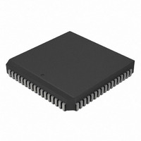
PIC18C801-I/L Microchip Technology, PIC18C801-I/L Datasheet - Page 46

PIC18C801-I/L
Manufacturer Part Number
PIC18C801-I/L
Description
IC,MICROCONTROLLER,8-BIT,PIC CPU,CMOS,LDCC,84PIN,PLASTIC
Manufacturer
Microchip Technology
Series
PIC® 18Cr
Datasheets
1.PIC16F616T-ISL.pdf
(8 pages)
2.PIC18C601-IL.pdf
(320 pages)
3.PIC18C601-IL.pdf
(10 pages)
4.PIC18C601-IL.pdf
(10 pages)
Specifications of PIC18C801-I/L
Rohs Compliant
YES
Core Processor
PIC
Core Size
8-Bit
Speed
25MHz
Connectivity
EBI/EMI, I²C, SPI, UART/USART
Peripherals
Brown-out Detect/Reset, LVD, POR, PWM, WDT
Number Of I /o
37
Program Memory Type
ROMless
Ram Size
1.5K x 8
Voltage - Supply (vcc/vdd)
4.2 V ~ 5.5 V
Data Converters
A/D 12x10b
Oscillator Type
External
Operating Temperature
-40°C ~ 85°C
Package / Case
84-PLCC
Processor Series
PIC18C
Core
PIC
Data Bus Width
8 bit
Data Ram Size
1.5 KB
Interface Type
3-Wire, I2C, SPI, USART
Maximum Clock Frequency
25 MHz
Number Of Programmable I/os
47
Number Of Timers
1 x 16 bit
Operating Supply Voltage
2 V to 5.5 V
Maximum Operating Temperature
+ 85 C
Mounting Style
SMD/SMT
3rd Party Development Tools
52715-96, 52716-328, 52717-734, 52712-325, EWPIC18
Development Tools By Supplier
DV164005, ICE4000, DV164136
Minimum Operating Temperature
- 40 C
On-chip Adc
10 bit
Lead Free Status / RoHS Status
Lead free / RoHS Compliant
For Use With
AC164310 - MODULE SKT FOR PM3 84PLCCXLT84L1 - SOCKET TRANSITION ICE 84PLCCAC174012 - MODULE SKT PROMATEII 84PLCC
Eeprom Size
-
Program Memory Size
-
Lead Free Status / Rohs Status
Details
Other names
PIC18C801-I/LR
PIC18C801-I/LR
PIC18C801I/L
PIC18C801-I/LR
PIC18C801I/L
Available stocks
Company
Part Number
Manufacturer
Quantity
Price
Company:
Part Number:
PIC18C801-I/L
Manufacturer:
MICROCHIP
Quantity:
12 000
Company:
Part Number:
PIC18C801-I/L
Manufacturer:
Microchip Technology
Quantity:
10 000
- PIC16F616T-ISL PDF datasheet
- PIC18C601-IL PDF datasheet #2
- PIC18C601-IL PDF datasheet #3
- PIC18C601-IL PDF datasheet #4
- Current page: 46 of 320
- Download datasheet (6Mb)
PIC18C601/801
4.4
The program counter (PC) specifies the address of the
instruction to fetch for execution. The PC is 21-bits
wide. The low byte is called the PCL register. This reg-
ister is readable and writable. The high byte is called
the PCH register. This register contains the PC<15:8>
bits and is not directly readable or writable. Updates to
the PCH register may be performed through the
PCLATH register. The upper byte is called PCU. This
register contains the PC<20:16> bits and is not directly
readable or writable. Updates to the PCU register may
be performed through the PCLATU register.
The PC addresses bytes in the program memory. To
prevent the PC from becoming misaligned with word
instructions, the LSb of the PCL is fixed to a value of ’0’.
The PC increments by 2 to address sequential instruc-
tions in the program memory.
The CALL,
instructions write to the program counter directly. For
these instructions, the contents of PCLATH and
PCLATU are not transferred to the program counter.
FIGURE 4-6:
DS39541A-page 46
OSC2/CLKOUT
PCL, PCLATH and PCLATU
(RC mode)
OSC1
RCALL,
Q4
PC
Q2
Q3
Q1
CLOCK/INSTRUCTION CYCLE
Q1
GOTO and program branch
Execute INST (PC-2)
Fetch INST (PC)
Q2
PC
Q3
Q4
Advance Information
Q1
Execute INST (PC)
Fetch INST (PC+2)
Q2
PC+2
The contents of PCLATH and PCLATU will be trans-
ferred to the program counter by an operation that
writes PCL. Similarly, the upper two bytes of the pro-
gram counter will be transferred to PCLATH and
PCLATU by an operation that reads PCL. This is useful
for computed offsets to the PC (See Section 4.8.1).
4.5
The clock input (from OSC1 or PLL output) is internally
divided by four to generate four non-overlapping
quadrature clocks, namely Q1, Q2, Q3 and Q4. Inter-
nally, the program counter (PC) is incremented every
Q1, the instruction is fetched from the program memory
and latched into the instruction register in Q4. The
instruction is decoded and executed during the follow-
ing Q1 through Q4. The clocks and instruction execu-
tion flow are shown in Figure 4-6.
Q3
Q4
Clocking Scheme/Instruction
Cycle
Q1
Execute INST (PC+2)
Fetch INST (PC+4)
Q2
PC+4
2001 Microchip Technology Inc.
Q3
Q4
Internal
Phase
Clock
Related parts for PIC18C801-I/L
Image
Part Number
Description
Manufacturer
Datasheet
Request
R

Part Number:
Description:
IC, 8BIT MCU, PIC18F, 40MHZ, LCC-44
Manufacturer:
Microchip Technology
Datasheet:

Part Number:
Description:
IC, 8BIT MCU, PIC18LF, 40MHZ, PLCC-64
Manufacturer:
Microchip Technology
Datasheet:

Part Number:
Description:
IC, 8BIT MCU, PIC18F, 64MHZ, TQFP-80
Manufacturer:
Microchip Technology
Datasheet:

Part Number:
Description:
MCU, MPU & DSP Development Tools CAN/LIN PICtail Plus Daughter Board
Manufacturer:
Microchip Technology
Datasheet:

Part Number:
Description:
IC, 8BIT MCU, PIC18F, 64MHZ, DIP-40
Manufacturer:
Microchip Technology
Datasheet:

Part Number:
Description:
IC, 8BIT MCU, PIC18LF, 40MHZ, PLCC-64
Manufacturer:
Microchip Technology
Datasheet:

Part Number:
Description:
IC, 8BIT MCU, PIC18F, 64MHZ, TQFP-64
Manufacturer:
Microchip Technology

Part Number:
Description:
IC, 8BIT MCU, PIC18F, 64MHZ, TQFP-80
Manufacturer:
Microchip Technology

Part Number:
Description:
8KB, Flash, 768bytes-RAM, 36I/O, 8-bit Family,nanowatt XLP 40 UQFN 5x5x0.5mm TUB
Manufacturer:
Microchip Technology
Datasheet:

Part Number:
Description:
8KB, Flash, 768bytes-RAM, 36I/O, 8-bit Family,nanowatt XLP 40 UQFN 5x5x0.5mm TUB
Manufacturer:
Microchip Technology

Part Number:
Description:
16KB, Flash, 768bytes-RAM, 36I/O, 8-bit Family,nanowatt XLP 40 UQFN 5x5x0.5mm TU
Manufacturer:
Microchip Technology
Datasheet:

Part Number:
Description:
16KB, Flash, 768bytes-RAM, 36I/O, 8-bit Family,nanowatt XLP 40 UQFN 5x5x0.5mm TU
Manufacturer:
Microchip Technology

Part Number:
Description:
32KB, Flash, 1536bytes-RAM, 36I/O, 8-bit Family,nanowatt XLP 40 UQFN 5x5x0.5mm T
Manufacturer:
Microchip Technology
Datasheet:

Part Number:
Description:
32KB, Flash, 1536bytes-RAM, 36I/O, 8-bit Family,nanowatt XLP 40 UQFN 5x5x0.5mm T
Manufacturer:
Microchip Technology

Part Number:
Description:
64KB, Flash, 3968bytes-RAM, 36I/O, 8-bit Family,nanowatt XLP 40 UQFN 5x5x0.5mm T
Manufacturer:
Microchip Technology
Datasheet:


