PIC18C801-I/L Microchip Technology, PIC18C801-I/L Datasheet - Page 197
PIC18C801-I/L
Manufacturer Part Number
PIC18C801-I/L
Description
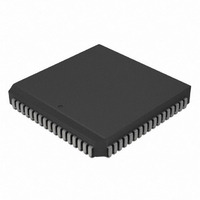
IC,MICROCONTROLLER,8-BIT,PIC CPU,CMOS,LDCC,84PIN,PLASTIC
Manufacturer
Microchip Technology
Series
PIC® 18Cr
Datasheets
1.PIC16F616T-ISL.pdf
(8 pages)
2.PIC18C601-IL.pdf
(320 pages)
3.PIC18C601-IL.pdf
(10 pages)
4.PIC18C601-IL.pdf
(10 pages)
Specifications of PIC18C801-I/L
Rohs Compliant
YES
Core Processor
PIC
Core Size
8-Bit
Speed
25MHz
Connectivity
EBI/EMI, I²C, SPI, UART/USART
Peripherals
Brown-out Detect/Reset, LVD, POR, PWM, WDT
Number Of I /o
37
Program Memory Type
ROMless
Ram Size
1.5K x 8
Voltage - Supply (vcc/vdd)
4.2 V ~ 5.5 V
Data Converters
A/D 12x10b
Oscillator Type
External
Operating Temperature
-40°C ~ 85°C
Package / Case
84-PLCC
Processor Series
PIC18C
Core
PIC
Data Bus Width
8 bit
Data Ram Size
1.5 KB
Interface Type
3-Wire, I2C, SPI, USART
Maximum Clock Frequency
25 MHz
Number Of Programmable I/os
47
Number Of Timers
1 x 16 bit
Operating Supply Voltage
2 V to 5.5 V
Maximum Operating Temperature
+ 85 C
Mounting Style
SMD/SMT
3rd Party Development Tools
52715-96, 52716-328, 52717-734, 52712-325, EWPIC18
Development Tools By Supplier
DV164005, ICE4000, DV164136
Minimum Operating Temperature
- 40 C
On-chip Adc
10 bit
Lead Free Status / RoHS Status
Lead free / RoHS Compliant
For Use With
AC164310 - MODULE SKT FOR PM3 84PLCCXLT84L1 - SOCKET TRANSITION ICE 84PLCCAC174012 - MODULE SKT PROMATEII 84PLCC
Eeprom Size
-
Program Memory Size
-
Lead Free Status / Rohs Status
Details
Other names
PIC18C801-I/LR
PIC18C801-I/LR
PIC18C801I/L
PIC18C801-I/LR
PIC18C801I/L
Available stocks
Company
Part Number
Manufacturer
Quantity
Price
Company:

Part Number:
PIC18C801-I/L
Manufacturer:
MICROCHIP
Quantity:
12 000
Company:
Part Number:
PIC18C801-I/L
Manufacturer:
Microchip Technology
Quantity:
10 000


The value in the ADRESH/ADRESL registers is not
modified for a Power-on Reset. The ADRESH/ADRESL
registers will contain unknown data after a Power-on
Reset.
After the A/D module has been configured as desired,
the selected channel must be acquired before the con-
version is started. The analog input channels must
have their corresponding TRIS bits selected as an
input. To determine acquisition time, see Section 17.1.
After this acquisition time has elapsed, the A/D conver-
sion can be started. The following steps should be fol-
lowed to do an A/D conversion:
1.
FIGURE 17-2:
2001 Microchip Technology Inc.
Configure the A/D module:
•
•
•
•
Configure analog pins, voltage reference
and digital I/O (ADCON1)
Select A/D input channel (ADCON0)
Select A/D conversion clock (ADCON2)
Turn on A/D module (ADCON0)
Legend: C
V
AIN
Rs
V
I
R
SS
C
R
LEAKAGE
T
PIN
IC
HOLD
SS
ANALOG INPUT MODEL
ANx
C
5 pF
PIN
= input capacitance
= threshold voltage
= leakage current at the pin due to
= interconnect resistance
= sampling switch
= sample/hold capacitance (from DAC)
= sampling switch resistance
various junctions
V
DD
Advance Information
V
V
T
T
= 0.6 V
= 0.6 V
I leakage
± 500 nA
2.
3.
4.
5.
6.
7.
R
IC
Configure A/D interrupt (if desired):
•
•
•
Wait the required acquisition time.
Start conversion:
•
Wait for A/D conversion to complete, by either:
•
•
Read A/D Result registers (ADRESH:ADRESL);
clear bit ADIF, if required.
For next conversion, go to step 1 or step 2, as
required. The A/D conversion time per bit is
defined as T
required before next acquisition starts.
1 k
Clear ADIF bit
Set ADIE bit
Set GIE bit
Set GO/DONE bit (ADCON0 register)
Polling for the GO/DONE bit to be cleared,
OR
Waiting for the A/D interrupt
V
SS
DD
Sampling
Switch
PIC18C601/801
6V
5V
4V
3V
2V
R
AD
SS
. A minimum wait of 2T
Sampling Switch
5 6 7 8 9 10 11
V
SS
C
HOLD
= 120 pF
DS39541A-page 197
( k )
AD
is
Related parts for PIC18C801-I/L
Image
Part Number
Description
Manufacturer
Datasheet
Request
R

Part Number:
Description:
IC, 8BIT MCU, PIC18F, 40MHZ, LCC-44
Manufacturer:
Microchip Technology
Datasheet:
Part Number:
Description:
IC, 8BIT MCU, PIC18LF, 40MHZ, PLCC-64
Manufacturer:
Microchip Technology
Datasheet:
Part Number:
Description:
IC, 8BIT MCU, PIC18F, 64MHZ, TQFP-80
Manufacturer:
Microchip Technology
Datasheet:

Part Number:
Description:
MCU, MPU & DSP Development Tools CAN/LIN PICtail Plus Daughter Board
Manufacturer:
Microchip Technology
Datasheet:

Part Number:
Description:
IC, 8BIT MCU, PIC18F, 64MHZ, DIP-40
Manufacturer:
Microchip Technology
Datasheet:

Part Number:
Description:
IC, 8BIT MCU, PIC18LF, 40MHZ, PLCC-64
Manufacturer:
Microchip Technology
Datasheet:
Part Number:
Description:
IC, 8BIT MCU, PIC18F, 64MHZ, TQFP-64
Manufacturer:
Microchip Technology
Part Number:
Description:
IC, 8BIT MCU, PIC18F, 64MHZ, TQFP-80
Manufacturer:
Microchip Technology

Part Number:
Description:
8KB, Flash, 768bytes-RAM, 36I/O, 8-bit Family,nanowatt XLP 40 UQFN 5x5x0.5mm TUB
Manufacturer:
Microchip Technology
Datasheet:
Part Number:
Description:
8KB, Flash, 768bytes-RAM, 36I/O, 8-bit Family,nanowatt XLP 40 UQFN 5x5x0.5mm TUB
Manufacturer:
Microchip Technology
Part Number:
Description:
16KB, Flash, 768bytes-RAM, 36I/O, 8-bit Family,nanowatt XLP 40 UQFN 5x5x0.5mm TU
Manufacturer:
Microchip Technology
Datasheet:
Part Number:
Description:
16KB, Flash, 768bytes-RAM, 36I/O, 8-bit Family,nanowatt XLP 40 UQFN 5x5x0.5mm TU
Manufacturer:
Microchip Technology
Part Number:
Description:
32KB, Flash, 1536bytes-RAM, 36I/O, 8-bit Family,nanowatt XLP 40 UQFN 5x5x0.5mm T
Manufacturer:
Microchip Technology
Datasheet:
Part Number:
Description:
32KB, Flash, 1536bytes-RAM, 36I/O, 8-bit Family,nanowatt XLP 40 UQFN 5x5x0.5mm T
Manufacturer:
Microchip Technology
Part Number:
Description:
64KB, Flash, 3968bytes-RAM, 36I/O, 8-bit Family,nanowatt XLP 40 UQFN 5x5x0.5mm T
Manufacturer:
Microchip Technology
Datasheet: