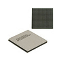
EP4SGX530HH35C2N Altera, EP4SGX530HH35C2N Datasheet - Page 522

EP4SGX530HH35C2N
Manufacturer Part Number
EP4SGX530HH35C2N
Description
IC STRATIX IV FPGA 530K 1152HBGA
Manufacturer
Altera
Series
Stratix® IV GXr
Datasheets
1.EP4SGX110DF29C3N.pdf
(80 pages)
2.EP4SGX110DF29C3N.pdf
(1154 pages)
3.EP4SGX110DF29C3N.pdf
(432 pages)
4.EP4SGX110DF29C3N.pdf
(22 pages)
5.EP4SGX110DF29C3N.pdf
(30 pages)
6.EP4SGX110DF29C3N.pdf
(72 pages)
7.EP4SGX530HH35C2N.pdf
(1145 pages)
Specifications of EP4SGX530HH35C2N
Number Of Logic Elements/cells
531200
Number Of Labs/clbs
21248
Total Ram Bits
27376
Number Of I /o
564
Voltage - Supply
0.87 V ~ 0.93 V
Mounting Type
Surface Mount
Operating Temperature
0°C ~ 85°C
Package / Case
1152-HBGA
Family Name
Stratix® IV
Number Of Logic Blocks/elements
531200
# Registers
424960
# I/os (max)
560
Process Technology
40nm
Operating Supply Voltage (typ)
900mV
Logic Cells
531200
Ram Bits
28033024
Operating Supply Voltage (min)
0.87V
Operating Supply Voltage (max)
0.93V
Operating Temp Range
0C to 85C
Operating Temperature Classification
Commercial
Mounting
Surface Mount
Pin Count
1152
Package Type
FCHBGA
Lead Free Status / RoHS Status
Lead free / RoHS Compliant
Number Of Gates
-
Lead Free Status / Rohs Status
Compliant
Available stocks
Company
Part Number
Manufacturer
Quantity
Price
- EP4SGX110DF29C3N PDF datasheet
- EP4SGX110DF29C3N PDF datasheet #2
- EP4SGX110DF29C3N PDF datasheet #3
- EP4SGX110DF29C3N PDF datasheet #4
- EP4SGX110DF29C3N PDF datasheet #5
- EP4SGX110DF29C3N PDF datasheet #6
- EP4SGX530HH35C2N PDF datasheet #7
- Current page: 522 of 1154
- Download datasheet (32Mb)
1–78
Stratix IV Device Handbook Volume 2: Transceivers
1
The rate match FIFO consists of a 20-word deep FIFO and necessary logic that controls
insertion and deletion of a skip character or ordered set, depending on the PPM
difference.
The rate match FIFO is mandatory and cannot be bypassed in the following functional
modes:
■
■
■
The rate match FIFO is optional in the following functional modes:
■
■
■
The rate match FIFO receives data from the word aligner (non-XAUI functional
modes) or deskew FIFO (XAUI functional mode) in the receiver datapath. It provides
the following status signals forwarded to the FPGA fabric:
■
■
■
■
The rate match FIFO status signals are not available in PCIe mode. These signals are
encoded on the pipestatus[2:0] signal in PCIe mode as specified in the PCIe
specification.
In PCIe mode, the rate match FIFO is capable of compensating up to ± 300 PPM (total
600 PPM) difference between the upstream transmitter and the local receiver. The
PCIe protocol requires the transmitter to send SKP ordered sets during IPGs, adhering
to rules listed in the base specification. The SKP ordered set is defined as a /K28.5/
COM symbol followed by three consecutive /K28.0/ SKP symbol groups. The PCIe
protocol requires the receiver to recognize a SKP ordered set as a /K28.5/ COM
symbol followed by one to five consecutive /K28.0/ SKP symbols.
The rate match FIFO operation is compliant to PCIe Base Specification 2.0. The rate
match operation begins after the synchronization state machine in the word aligner
indicates synchronization is acquired by driving the rx_syncstatus signal high. The
rate match FIFO looks for the SKP ordered set and deletes or inserts SKP symbols as
necessary to prevent the rate match FIFO from overflowing or under-running.
PCIe
XAUI
GIGE
Basic single-width
Basic double-width
SRIO
rx_rmfifodatainserted—indicates insertion of a skip character or ordered set
rx_rmfifodatadeleted—indicates deletion of a skip character or ordered set
rx_rmfifofull—indicates rate match FIFO full condition
rx_rmfifoempty—indicates rate match FIFO empty condition
Rate Match FIFO in PCIe Mode
Chapter 1: Transceiver Architecture in Stratix IV Devices
February 2011 Altera Corporation
Transceiver Block Architecture
Related parts for EP4SGX530HH35C2N
Image
Part Number
Description
Manufacturer
Datasheet
Request
R

Part Number:
Description:
CYCLONE II STARTER KIT EP2C20N
Manufacturer:
Altera
Datasheet:

Part Number:
Description:
CPLD, EP610 Family, ECMOS Process, 300 Gates, 16 Macro Cells, 16 Reg., 16 User I/Os, 5V Supply, 35 Speed Grade, 24DIP
Manufacturer:
Altera Corporation
Datasheet:

Part Number:
Description:
CPLD, EP610 Family, ECMOS Process, 300 Gates, 16 Macro Cells, 16 Reg., 16 User I/Os, 5V Supply, 15 Speed Grade, 24DIP
Manufacturer:
Altera Corporation
Datasheet:

Part Number:
Description:
Manufacturer:
Altera Corporation
Datasheet:

Part Number:
Description:
CPLD, EP610 Family, ECMOS Process, 300 Gates, 16 Macro Cells, 16 Reg., 16 User I/Os, 5V Supply, 30 Speed Grade, 24DIP
Manufacturer:
Altera Corporation
Datasheet:

Part Number:
Description:
High-performance, low-power erasable programmable logic devices with 8 macrocells, 10ns
Manufacturer:
Altera Corporation
Datasheet:

Part Number:
Description:
High-performance, low-power erasable programmable logic devices with 8 macrocells, 7ns
Manufacturer:
Altera Corporation
Datasheet:

Part Number:
Description:
Classic EPLD
Manufacturer:
Altera Corporation
Datasheet:

Part Number:
Description:
High-performance, low-power erasable programmable logic devices with 8 macrocells, 10ns
Manufacturer:
Altera Corporation
Datasheet:

Part Number:
Description:
Manufacturer:
Altera Corporation
Datasheet:

Part Number:
Description:
Manufacturer:
Altera Corporation
Datasheet:

Part Number:
Description:
Manufacturer:
Altera Corporation
Datasheet:

Part Number:
Description:
CPLD, EP610 Family, ECMOS Process, 300 Gates, 16 Macro Cells, 16 Reg., 16 User I/Os, 5V Supply, 25 Speed Grade, 24DIP
Manufacturer:
Altera Corporation
Datasheet:


